Rectifier circuit, and contactless power supply device

a technology of rectifier circuit and contactless power supply, which is applied in the direction of electric variable regulation, process and machine control, instruments, etc., can solve the problems of increasing power consumption and power loss of vtpid, and achieve the effect of improving power supply capability and low power loss

Active Publication Date: 2018-08-21
PANASONIC SEMICON SOLUTIONS CO LTD
View PDF24 Cites 3 Cited by
  • Summary
  • Abstract
  • Description
  • Claims
  • Application Information

AI Technical Summary

Benefits of technology

[0017]To mount the circuit illustrated in FIG. 13 on an IC chip for a smart card and for an RFID tag, the IC chip needs to be produced through the CMOS process so that the IC chip is produced at low cost. Accordingly, bipolar transistors 68 and 69 need to be replaced with N-channel MOS transistors. FIG. 14 illustrates a circuit configured by replacing bipolar transistors 68 and 69 of the circuit illustrated in FIG. 13 with N-channel MOS transistors. Generally, a relative variation in threshold voltages of two MOS transistors is greater than a relative variation in threshold voltages of two bipolar transistors. Therefore, with bipolar transistors replaced with MOS transistors, an input-offset voltage of voltage comparator 62 increases, and when a voltage across terminal A is less than a voltage across terminal K, a reverse current flowing from terminal K to terminal A is not interrupted, producing power losses. Reducing a variation in threshold voltages of the MOS transistors, which variation causes the power losses, requires gate areas of the MOS transistors to be increased. Consequently, gate capacitances of N-channel MOS transistors 70 and 71 increase, and when an AC voltage is applied to terminal K, a delay in a response of voltage comparator 62 increases. The delay in the response of voltage comparator 62 generates a reverse current, leading to power losses.
[0019]The present disclosure provides a rectifier circuit that has low power losses and that operates at high frequencies, and a contactless power supply device, typified by a smart card and an RFID tag, which has an improved power supply capability achieved by mounting the rectifier circuit to a power supply circuit.
[0022]The present disclosure enables a rectifier circuit to have low power losses and to operate at high frequencies, and a contactless power supply device to have an improved power supply capability.

Problems solved by technology

Generally, increases in a speed of a CPU and in a speed of access to a memory are accompanied by an increase in power consumption, which requires such smart cards to draw power from an electromagnetic field more efficiently.
In the circuit of FIG. 12, however, for current Id to flow from terminal A to terminal K, a voltage across terminal A is required to be increased by threshold voltage Vtp of the MOS transistor relative to a voltage across terminal K, resulting in a power loss of Vtp×Id.

Method used


Image

  • Rectifier circuit, and contactless power supply device
  • Rectifier circuit, and contactless power supply device
  • Rectifier circuit, and contactless power supply device

Examples


first exemplary embodiment

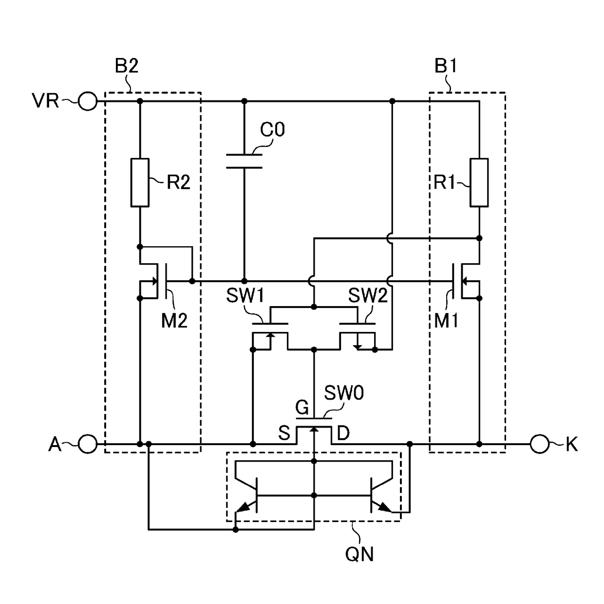
[0037]FIG. 1 illustrates an example configuration of a rectifier circuit according to a first exemplary embodiment of the present disclosure. The rectifier circuit of FIG. 1 includes three terminals A, K, VR and is formed of N-channel MOS transistor SW0 as a current switching unit, voltage comparator B1, and reference voltage generator B2. N-channel MOS transistor SW1 operating as a switch is connected between a source and a gate of N-channel MOS transistor SW0. P-channel MOS transistor SW2 operating as a switch is connected between the gate of N-channel MOS transistor SW0 and terminal VR. N-channel MOS transistor SW0 is formed on a triple well, with a back gate connected to the source and to an N-well substrate. QN indicates a parasitic bipolar transistor incorporated inside N-channel MOS transistor SW0.

[0038]Reference voltage generator B2 is formed of N-channel MOS transistor M2 in which a gate and a drain are commonly connected, and resistor R2. Resistor R2 is connected between t...

second exemplary embodiment

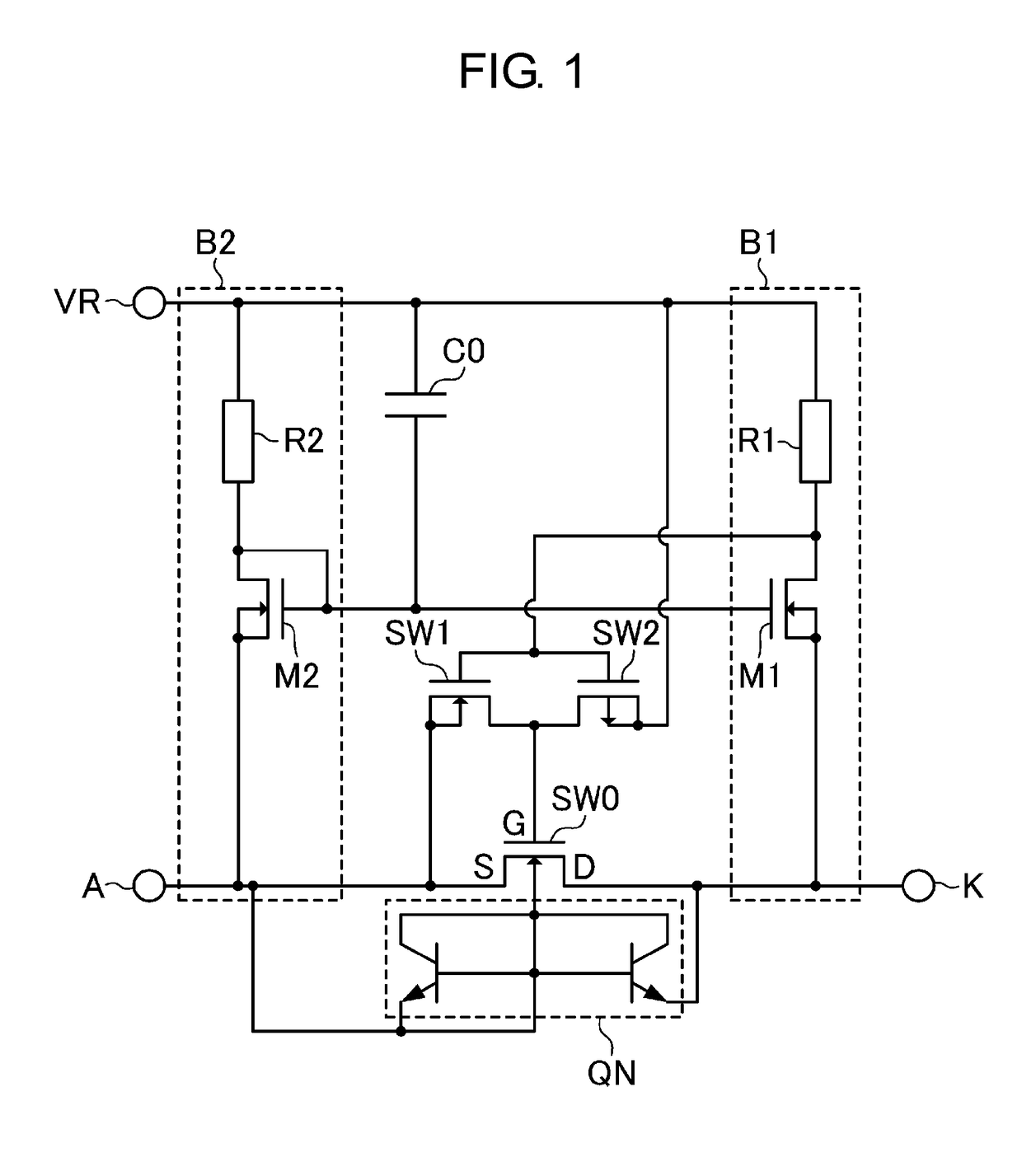
[0042]FIG. 2 illustrates an example configuration of a rectifier circuit according to a second exemplary embodiment of the present disclosure. The rectifier circuit of FIG. 2 includes three terminals A, K, VR, and is formed of P-channel MOS transistor SW0 as a current switching unit, voltage comparator B1, and reference voltage generator B2. P-channel MOS transistor SW1 operating as a switch is connected between a source and a gate of P-channel MOS transistor SW0, and N-channel MOS transistor SW2 operating as a switch is connected between the gate of P-channel MOS transistor SW0 and terminal VR. A back gate of P-channel MOS transistor SW0 is connected to the source. QP indicates a parasitic bipolar transistor incorporated inside P-channel MOS transistor SW0.

[0043]Reference voltage generator B2 is formed of P-channel MOS transistor M2 in which a gate and a drain are commonly connected, and resistor R2. Resistor R2 is connected between terminal VII and the drain of P-channel MOS trans...

third exemplary embodiment

[0047]FIG. 3 illustrates an example configuration of a rectifier circuit according to a third exemplary embodiment of the present disclosure. In the rectifier circuit of FIG. 3, resistor R1 and resistor R2, which are used in the rectifier circuit of FIG. 1, are respectively replaced with P-channel MOS transistors M3 and M4 each operating as a constant current source. The rectifier circuit of FIG. 3 differs from the rectifier circuit of FIG. 1 in that: a drain and a source of N-channel MOS transistor SW4 are respectively connected to a source and a back gate of N-channel MOS transistor SW0; a drain and a source of N-channel MOS transistor SW3 are respectively connected to a drain and the back gate of N-channel MOS transistor SW0; an N-well substrate of N-channel MOS transistor SW0 formed on a triple well is connected to terminal VR; a gate of N-channel MOS transistor SW0 is connected to a gate of N-channel MOS transistor SW3; and a comparative output terminal of voltage comparator B1...


PUM


Abstract

The rectifier circuit includes: three terminals A, K, VR; voltage comparator including a positive input terminal, a negative input terminal, and a comparative output terminal; current switching unit including source terminal, drain terminal, and control terminal; first switching unit that conducts or cuts off between source terminal and control terminal of the current switching unit; second switching unit that conducts or cuts off between control terminal of the current switching unit and terminal VR; and reference voltage generator that uses terminal A and terminal VR as input terminals, and includes a voltage output terminal. The voltage output terminal of reference voltage generator is connected to the negative input terminal of the voltage comparator, terminal K is connected to the positive input terminal of voltage comparator, and current flow between first switching unit and second switching unit is exclusively allowed or interrupted by a signal output from the comparative output terminal of voltage comparator).

Description

BACKGROUND1. Technical Field[0001]The present disclosure relates to a rectifier circuit, in particular, to a rectifier circuit including a current switching unit that allows a current to flow in one direction in response to an output signal from a voltage comparator and interrupts a reverse current, and to a contactless power supply device that includes a power supply part having the rectifier circuit.2. Description of the Related Art[0002]Smart cards and RFID (Radio Frequency Identifier) tags which have no battery as a power source communicate by drawing, via an antenna, power from an electromagnetic field produced by a communication device.[0003]In recent years, there is a trend that smart cards store more biological information than ever on a non-volatile memory to provide secure authentication. To enable such smart cards to process more data in a short time, a faster internal CPU (Central Processing Unit) and faster access to a memory have been demanded. Generally, increases in ...

Claims


Application Information

Patent Timeline
Patent Type & Authority Patents(United States)
IPC IPC(8): H02J50/10H02M3/335H02J50/12H02M7/217
CPCH02J50/12H02J50/10H02M7/217H02M3/33592Y02B70/1475H02J50/80H02J7/00034H02J7/007Y02B70/10Y02B40/00
Inventor MORIKAWA, HIROYASU
Owner PANASONIC SEMICON SOLUTIONS CO LTD
Why Eureka
Try Eureka