

TFT substrate, display device and manufacturing method
a manufacturing method and substrate technology, applied in the field of display technology, can solve the problem that traditional circuit design cannot meet the requirement for a higher ppi, and achieve the effect of saving layout space and realizing higher ppi
- Summary
- Abstract
- Description
- Claims
- Application Information
AI Technical Summary
Benefits of technology
Problems solved by technology
Method used
Image

Examples
first embodiment
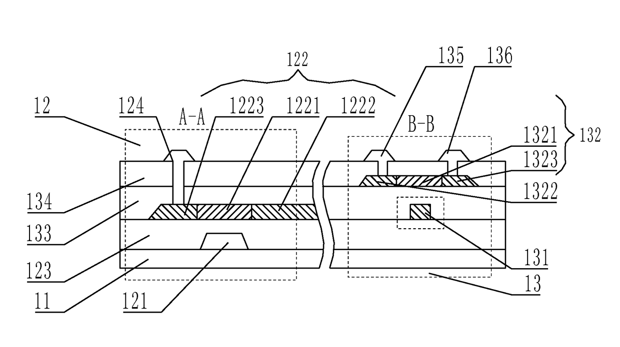
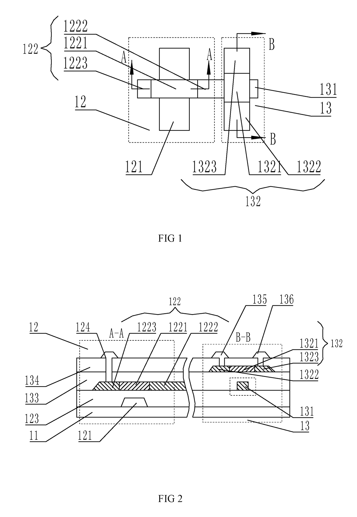
[0063]In the TFT substrate of the present invention, through a layout method that extending the first doping region 1222 of the first TFT structure 12 to and inside the second TFT structure 13, and functioning as the second gate pattern 131 of the second TFT structure 13, saving the layout space, and beneficial for a realization of higher PPI.
second embodiment
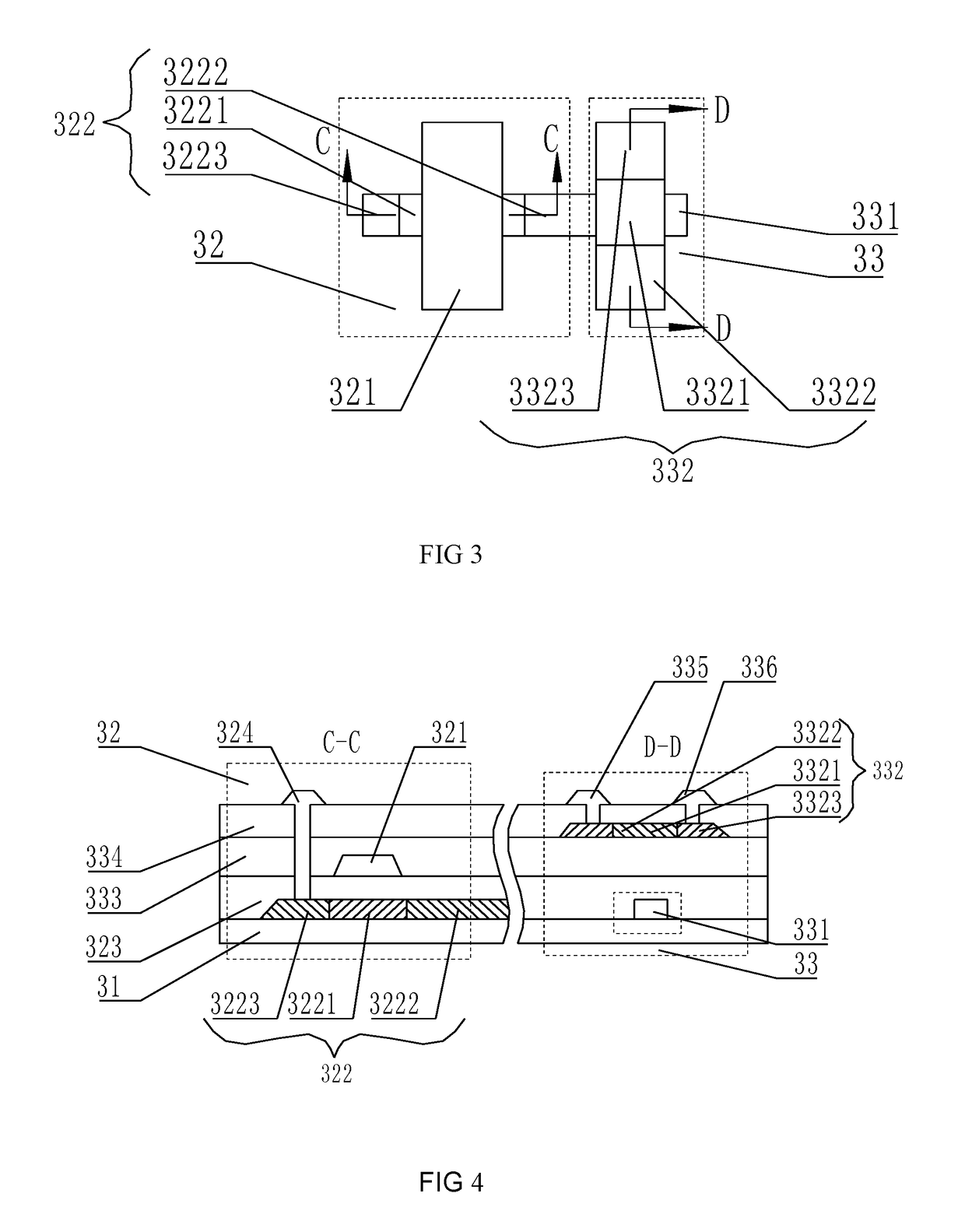
[0064]With reference to FIG. 3, and FIG. 3 is a schematic top view structure of a TFT substrate of the present invention. In the present embodiment, the embodiment includes a substrate 31, a first TFT structure 32 and a second TFT structure 33 which are formed on the substrate 31. Wherein, the first TFT structure 32 includes a first gate pattern 321 and a first semiconductor pattern 322. The first semiconductor pattern 322 is divided into a first channel region 3221 and a first doping region 3222 and a second doping region 3223 located at two sides of the first channel region 3221. Wherein, the first channel region 3221 is disposed corresponding to the first gate pattern 321 so as to form a first conductive channel under the function of the first gate pattern 321. The first doping region 3222 is extended to and inside the second TFT structure 33 and functions as a second gate pattern 331 of the second TFT structure 33.
[0065]Wherein, the second TFT structure 33 includes a second semi...
PUM
 Abstract
Description
Claims
Application Information