Detector device for detection of a spectral portion for a microscope

a technology of spectral portion and detector device, which is applied in the field of detector device for microscope, can solve the problem of wasting pinholes, and achieve the effects of reducing transverse chromatic aberration, small focal spot, and complementary optical properties

Active Publication Date: 2018-11-20
CARL ZEISS MICROSCOPY GMBH
View PDF19 Cites 4 Cited by
  • Summary
  • Abstract
  • Description
  • Claims
  • Application Information

AI Technical Summary

Benefits of technology

[0015]It is possible for the sensor to have a sensitive area in the region of more than 0.1 mm2 or more than 1 mm2 or more than 100 mm2. However, in various embodiments, it is also possible to obtain focusing on a comparatively small sensor. By way of example, the sensor may have a sensitive area of less than 0.1 mm2. Preferably, the sensor may have a sensitive area of less than 0.05 mm2. Particularly preferably, the sensor may have a sensitive area of less than 0.02 mm2. By way of example, the focusing optical unit may be configured to focus the beam path of the spectral portion of the light onto the sensitive area or detection area of the sensor. Thus, the focal spot may have substantially the same dimensions as the sensitive area of the sensor. As a result, use may also be made of those sensors which have a comparatively high sensitivity, e.g. APDs, APD arrays or single photon avalanche diode (SPAD) array sensors, electron multiplying charge-coupled device (EMCC) sensors, etc. The imaging quality may be improved.
[0034]Thus, in general, it is possible for more than one spectral portion to be selected by the selection element. As a result, spectrally selective imaging for different spectral portions of the light may be effected comparatively quickly. It is possible for the focusing optical unit and the further focusing optical unit to be configured accordingly. As a result, it may be possible to obtain effects for the further focusing optical unit, which effects may be obtained for the focusing optical unit as described above.

Problems solved by technology

However, the pinhole may be expendable.

Method used


Image

  • Detector device for detection of a spectral portion for a microscope
  • Detector device for detection of a spectral portion for a microscope
  • Detector device for detection of a spectral portion for a microscope

Examples


Embodiment Construction

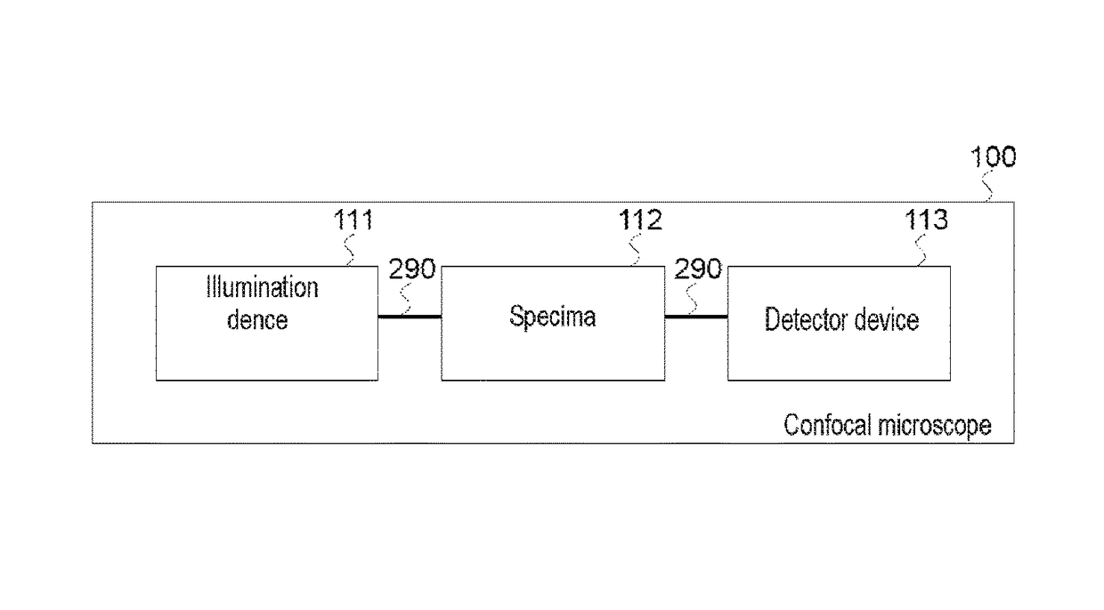
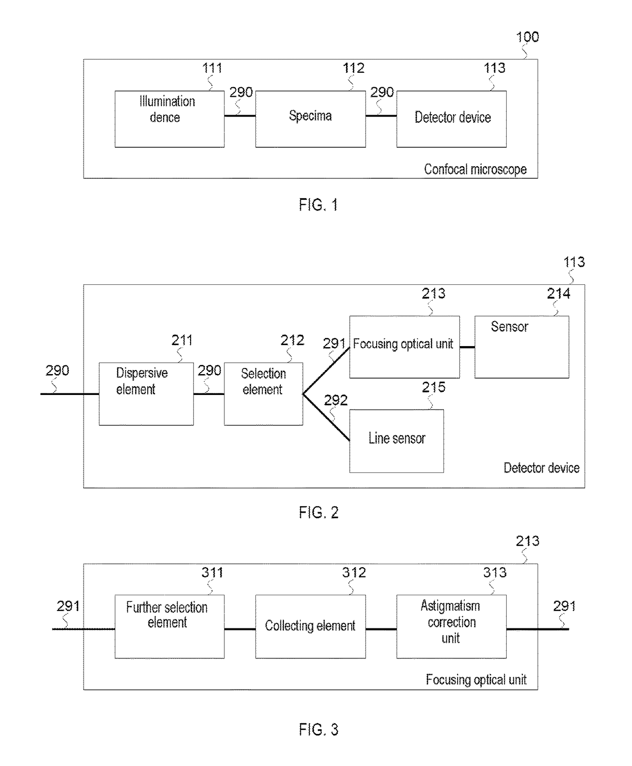
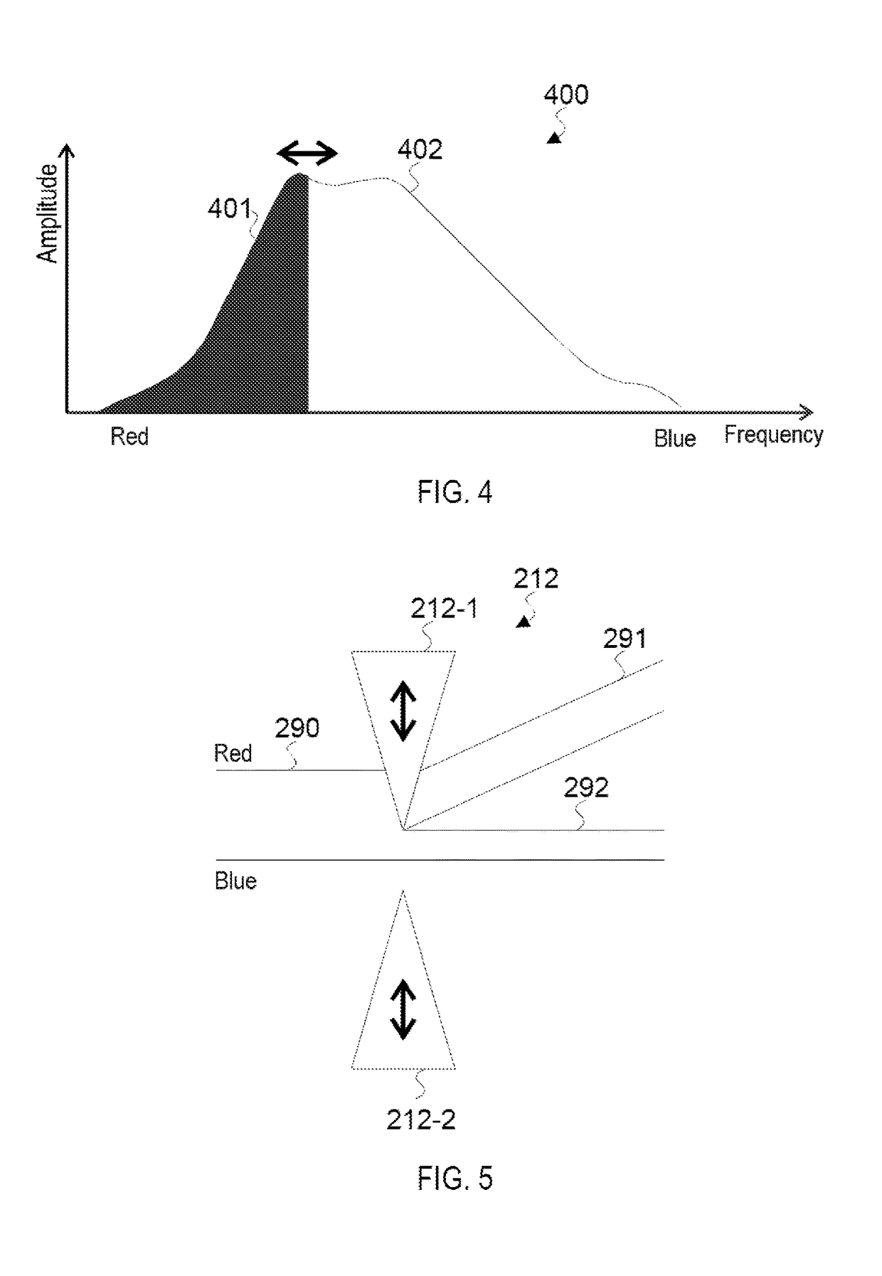
[0048]The present invention is explained in greater detail below on the basis of preferred embodiments with reference to the drawings. In the figures, identical reference signs denote identical or similar elements. The figures are schematic representations of different embodiments of the invention. Elements depicted in the figures are not necessarily depicted true to scale. Rather, the different elements illustrated in the figures are reproduced in such a way that their function and general purpose become comprehensible to the person skilled in the art. Connections and couplings between functional units and elements as depicted in the figures may also be implemented as indirect connection or coupling. A connection or coupling may be implemented in a wired or wireless manner. Functional units may be implemented as hardware, software or a combination of hardware and software.

[0049]Below, a detector device for selecting one or more spectral portions is illustrated. By way of example, t...


PUM

PropertyMeasurementUnit
sensitive areaaaaaaaaaaa

Abstract

A detection device for a microscope comprises a dispersive element in the beam path of light and a selection element. The selection element separates a beam path of a spectral portion of the light from the beam path of the light. The detector device furthermore comprises a focusing optical unit configured to focus the beam path of the spectral portion of the light onto a sensor. By way of example, the microscope may be a confocal microscope.

Description

TECHNICAL FIELD[0001]Various embodiments of the invention relate to a detector device for a microscope. In particular, various embodiments of the invention relate to a detector device which comprises a focusing optical unit arranged in the beam path of a spectral portion of light and configured to focus the beam path of the spectral portion of the light onto a sensor.BACKGROUND OF THE INVENTION[0002]In microscopy, there is a need for particularly high sensitivities of sensors for generating signals. In this way, an imaging quality may improve. Conventional large-area detectors, such as e.g. photomultipliers (PMTs), have a quantum efficiency of approximately 20%-50%, provided that these are, for example, implemented by means of GaAsP anodes. Such detectors have comparatively large sensitive areas (detection area) of the order of several mm2 or several tens of mm2.[0003]In principle, sensors with a relatively high sensitivity are known. By way of example, avalanche photodiodes (APDs) ...

Claims


Application Information

Patent Timeline
Patent Type & Authority Patents(United States)
IPC IPC(8): G01J3/28G01J3/44G01N21/64G01J3/02G01J3/14G01J3/18G02B27/00G02B21/36G02B21/16
CPCG01J3/4406G01J3/021G01J3/0208G01J3/14G01J3/18G02B21/16G02B21/361G02B27/0025G01N21/6458G01N2201/068G01N2021/6421G01J3/36G02B21/0064G02B21/0076G02B27/1013G02B27/126
Inventor SHAFER, DAVIDANHUT, TIEMOWALD, MATTHIAS
Owner CARL ZEISS MICROSCOPY GMBH
Why Eureka
Try Eureka