Organic light-emitting pixel including four sub-pixels having adjusted microcavity distances

a light-emitting pixel and organic technology, applied in the field of display technologies, can solve the problems of inconvenient cleaning of fmms, fmms may be difficult to manufacture for smaller aperture widths, and the prominentness of existing fmm technology, so as to improve the fabrication yield of the corresponding oled display panel and reduce the difficulty of fabrication

Active Publication Date: 2018-11-20
BOE TECH GRP CO LTD
View PDF12 Cites 3 Cited by
  • Summary
  • Abstract
  • Description
  • Claims
  • Application Information

AI Technical Summary

Benefits of technology

[0006]The present invention at least partially addresses the above problems in the prior art. The present disclosure provides an OLED pixel or organic light-emitting pixel with a plurality of subpixels, a display panel and a display apparatus containing the OLED pixel, and a method for forming the OLED pixel. By using the OLED pixel and method for forming the OLED pixel, the transparent ITO electrode corresponding to each microcavity may be formed to have a same thickness without additional etching process. Meanwhile, the OLED pixel may be configured to emit light of at least three colors. Fabrication difficulty can be reduced and the OLED pixel may emit light with desired color. Fabrication yield of the corresponding OLED display panel can be improved.

Problems solved by technology

However, because of the demand for higher resolution, pixels or subpixels with smaller sizes are preferred in display panels, and problems in existing FMM technology may become prominent.
For example, FMMs may be difficult to manufacture for smaller aperture widths.
It may also be inconvenient to clean the FMMs.
Additionally, in a deposition process, it may be difficult to align FMMs, and the FMMs may expand at high temperatures and / or low vacuum.
These problems may cause color mixing between different pixels or subpixels in the display panel and the resolution of the display panel may be adversely affected.
In such array substrate, the indium tin oxide (ITO) electrode corresponding to each microcavity may be hard to etch to a desired thickness or the etching may be hard to control.
As a result, cavity lengths of the microcavities may vary from design and the fabrication of the AMOLED array substrate may be difficult.

Method used


Image

  • Organic light-emitting pixel including four sub-pixels having adjusted microcavity distances
  • Organic light-emitting pixel including four sub-pixels having adjusted microcavity distances
  • Organic light-emitting pixel including four sub-pixels having adjusted microcavity distances

Examples


Embodiment Construction

[0038]For those skilled in the art to better understand the technical solution of the invention, reference will now be made in detail to exemplary embodiments of the invention, which are illustrated in the accompanying drawings. Wherever possible, the same reference numbers will be used throughout the drawings to refer to the same or like parts.

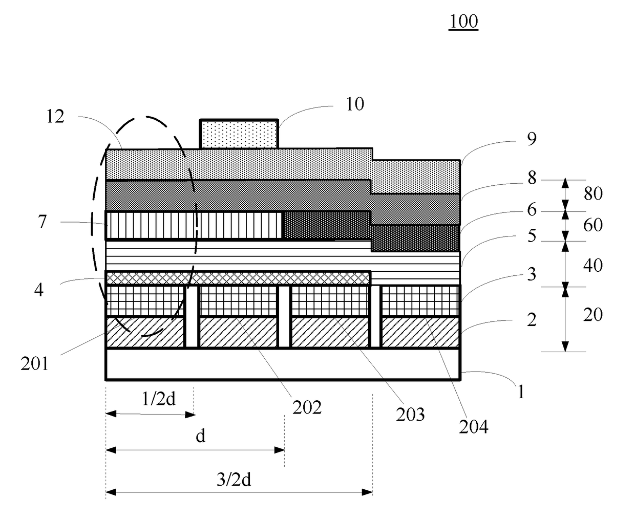
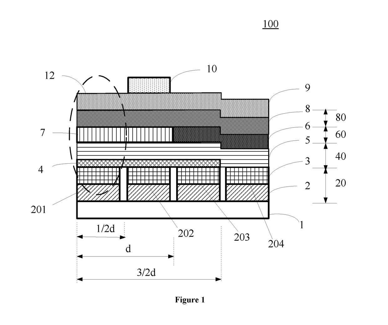
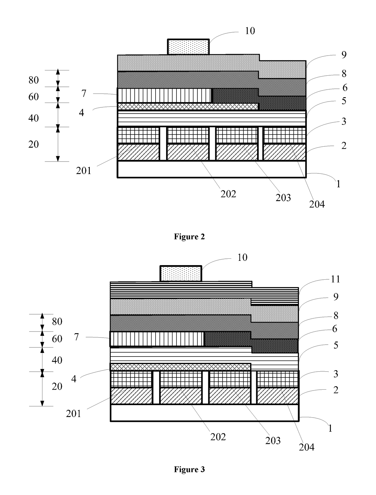
[0039]One aspect of the present disclosure provides an OLED pixel.

[0040]FIG. 1 illustrates an exemplary OLED pixel 100. The OLED pixel 100 may include a plurality of subpixels. The OLED pixel may enable subpixel with smaller sizes or widths to be fabricated using existing FMM technology. The OLED pixel in FIG. 1 may include a substrate 1, a first electrode layer 20, a first functional layer 40, a light-emitting layer 60, a second functional layer 80, a second electrode layer 9, and a color conversion layer 10.

[0041]In the OLED pixel, the first electrode layer 20 may be formed on the substrate 1. The first functional layer 40 may be formed on ...


PUM


Abstract

The present disclosure provides an organic light-emitting pixel with four subpixels formed in two groups, each group having two adjacent subpixels. The organic light-emitting pixel includes a first electrode layer formed on a substrate, including a plurality of first electrodes, each first electrode corresponding to one of the subpixels; a second electrode layer; and a first functional layer corresponding to three of the four subpixels. The first function layer is configured to adjust a distance between a first electrode and the second electrode layer. The organic light-emitting pixel also includes a light-emitting layer including a first portion and a second portion, the first portion corresponding to one of the two groups of subpixels and the second portion corresponding to another one of the two groups of subpixels, respectively.

Description

[0001]This application is a national phase entry under 35 U.S.C. § 371 of International Application No. PCT / CN2015 / 089659, filed on Sep. 15, 2015. The above enumerated patent application is incorporated by reference herein in its entirety.FIELD OF THE INVENTION[0002]The present invention generally relates to the display technologies and, more particularly, relates to an organic light-emitting pixel, a display panel and a display apparatus containing the same, and a method for forming the same.BACKGROUND[0003]Organic light-emitting diode (OLED) display products have been widely used in everyday life. The active-matrix organic light-emitting diode (AMOLED) display technologies enable OLED display products with lower costs, lower power consumptions, and larger sizes. In existing AMOLED technologies, there are several ways to form and pattern the organic layers. For example, the organic layers are often formed by vacuum evaporation. Shadow masks, i.e., fine metal masks (FMMs), are often...

Claims


Application Information

Patent Timeline
Patent Type & Authority Patents(United States)
IPC IPC(8): H01L29/08H01L51/56H01L27/32H01L51/50H01L51/52
CPCH01L27/3276H01L27/322H01L27/3213H01L51/5056H01L51/5203H01L51/5265H01L51/56H01L51/5072H01L2251/558H01L2227/323H10K59/351H10K50/15H10K50/16H10K50/852H10K71/00H10K2102/351H10K59/131H10K50/805H10K59/38H10K59/1201
Inventor YAN, GUANGWU, CHANG YEN
Owner BOE TECH GRP CO LTD
Why Eureka
Try Eureka