Dynamic random access memory array, semiconductor layout structure and fabrication method thereof

a random access memory and array technology, applied in the field of dynamic random access memory arrays, semiconductor layout structures and fabrication methods thereof, can solve the problems of ics complexity and performance, far exceeding the original expectations, and lowering the price of ics, so as to reduce the difficulty of fabrication, relieve the problem of high on-resistance, and reduce the effect of turn-on voltag

Active Publication Date: 2020-09-03
CHANGXIN MEMORY TECH INC
View PDF0 Cites 0 Cited by
  • Summary
  • Abstract
  • Description
  • Claims
  • Application Information

AI Technical Summary

Benefits of technology

[0036]In the DRAM array, the semiconductor layout structure and the method of the present disclosure, the active areas are arranged in such an array that adjacent active areas in each single column have different widths and that a direction of the columns intersects a direction in which the active areas extend. As a result, fabrication difficulty is reduced, a basis is provided for subsequent module fabrication, and the high turn-on voltage and high on-resistance problems are relieved.
[0037]Further, capacitors formed on the basis of the above have different capacitances due to different charge storage capacities of the active areas with different widths. As a result, multiple levels of storage ability are achieved, thus improving device performance.

Problems solved by technology

The performance and complexity of ICs have far exceeded the original expectations.
Increasing circuit density not only improves ICs' complexity and performance, but also lowers the price of the ICs.
To further shrink the feature size of IC components is challenging because every process involved in IC fabrication has a limit.
In addition, traditional processes and materials can hardly keep up with the increasingly high demands of IC design.
Memory size scale-down is a very challenging task because it is hard to scale down the size of memory cell without compromising the memory capacity per unit area.
This issue hinders the development of high-density memories.
Existing DRAMs have many issues that limit their performance, such as high turn-on voltage and large on-resistance.

Method used


Image

  • Dynamic random access memory array, semiconductor layout structure and fabrication method thereof
  • Dynamic random access memory array, semiconductor layout structure and fabrication method thereof
  • Dynamic random access memory array, semiconductor layout structure and fabrication method thereof

Examples


Embodiment Construction

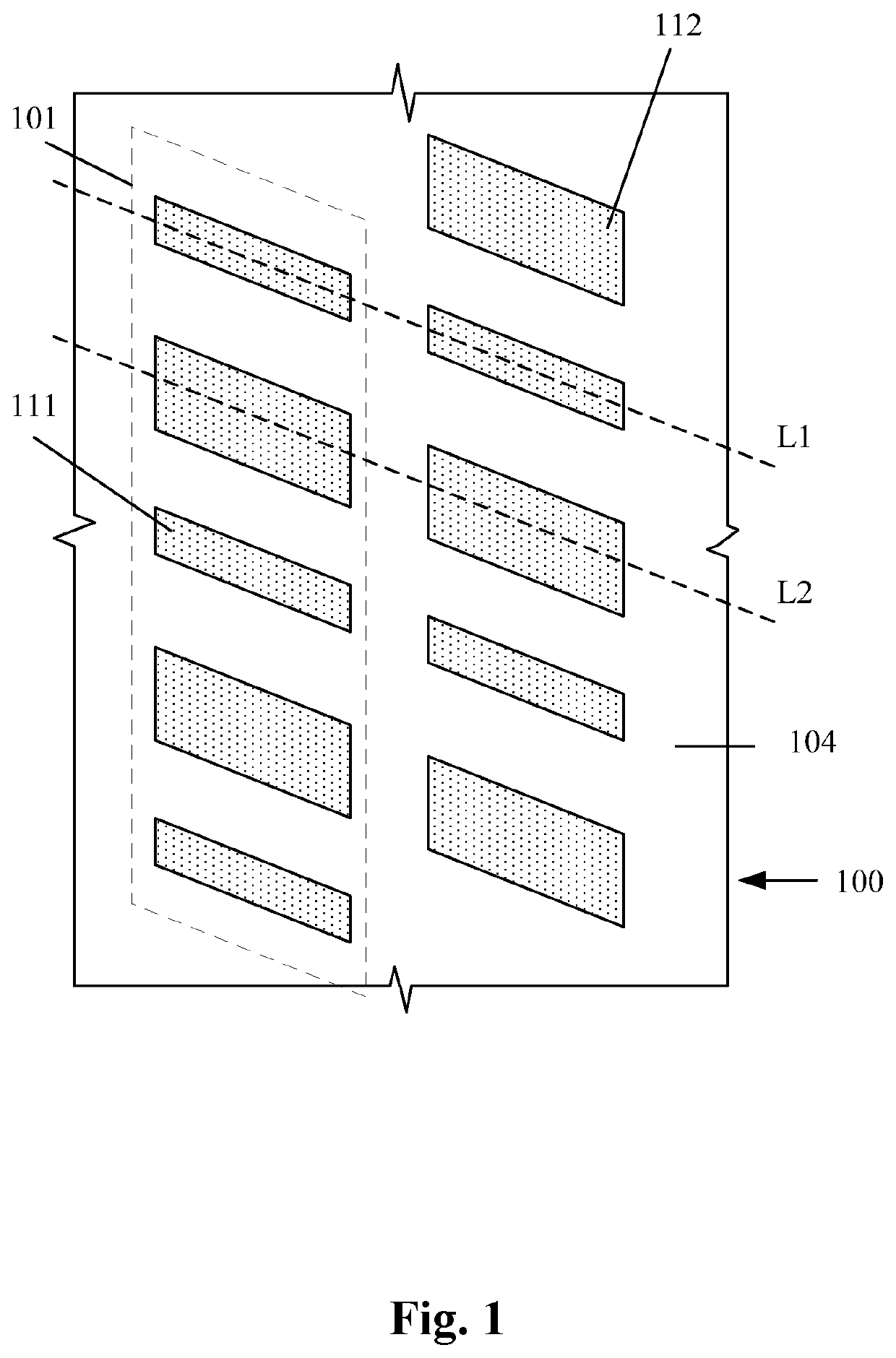
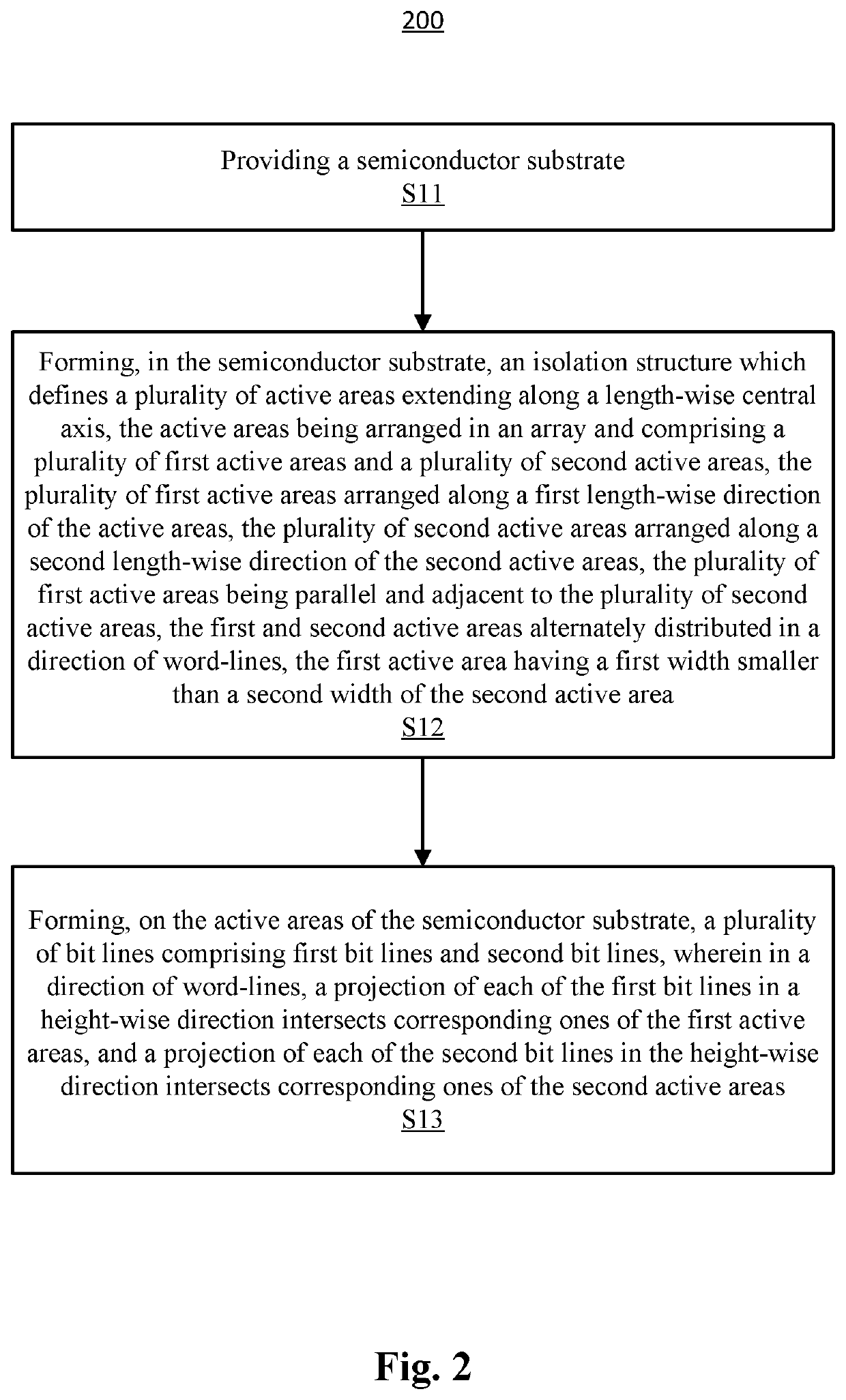
[0054]Dynamic random access memory (DRAM) arrays, semiconductor layout structure therefor and fabrication methods thereof according to the present disclosure will be described in greater detail below with reference to the accompanying drawings which provide preferred embodiments of the present disclosure. Those skilled in the art can make changes to the embodiments disclosed herein while still obtaining the beneficial results thereof. Therefore, the following description shall be construed in accordance with what is widely known by those skilled in the art, and should not be construed as limiting the scope of the present disclosure.

[0055]In the following description, when any layer (or film), region, pattern or structure is described as being “on,”“over,” (or overlying) a substrate, another layer (or film), another region, a welding pad and / or another pattern, the layer, region, pattern or structure may be disposed directly on the substrate, the other layer (or film), the other regi...


PUM


Abstract

A semiconductor layout structure for a dynamic random access memory (DRAM) array, comprising an isolation structure and a plurality of active areas situated in a semiconductor substrate, each of the active areas extending along a length-wise central axis. The isolation structure is situated among the active areas. The active areas are arranged in an array and comprise a plurality of first active areas and a plurality of second active areas. The first active areas are arranged along a first length-wise direction of the active areas. The second active areas are arranged along a second length-wise direction of the active areas. The first active areas are parallel and adjacent to the second active areas, and the first and second active areas are alternately distributed in a direction of word-lines. The first active area having a first width smaller than a second width of the second active area.

Description

CROSS-REFERENCE TO RELATED APPLICATIONS[0001]This application is a continuation application of International Patent Application No. PCT / CN2018 / 118069, filed on Nov. 29, 2018, which claims priority to China Patent Application No. 201711227178.X, filed with the China Patent Office on Nov. 29, 2017 and entitled “DYNAMIC RANDOM ACCESS MEMORY ARRAY, SEMICONDUCTOR LAYOUT STRUCTURE AND FABRICATION METHOD THEREOF.” The above-referenced applications are incorporated herein by reference in their entirety.TECHNICAL FIELD[0002]The present disclosure relates to the field of semiconductor technology and, in particular, to a dynamic random access memory (DRAM) array, a semiconductor layout structure and a fabrication method thereof.BACKGROUND[0003]Integrated circuits (ICs) have evolved from integrating dozens of components on a single chip to integrating millions of components. The performance and complexity of ICs have far exceeded the original expectations. To further enhance complexity and circ...

Claims


Application Information

Patent Timeline
Patent Type & Authority Applications(United States)
IPC IPC(8): G11C7/12G11C8/14H01L27/108
CPCG11C7/12H01L27/10885G11C8/14H01L27/1085H01L27/10823H01L23/50H10B69/00H10B12/31H10B12/488H10B12/09H10B12/50H10B12/03H10B12/34H10B12/482
Inventor LIU, CHIH CHENG
Owner CHANGXIN MEMORY TECH INC
Why Eureka
Try Eureka