

Electro-optical device, electronic apparatus, and method of driving electro-optical device
a technology of electrooptical devices and electronic devices, applied in static indicating devices, instruments, electroluminescent light sources, etc., can solve problems such as insufficient compensation in the compensation period, and achieve the effect of speeding up the compensation operation
Active Publication Date: 2018-12-11
SEIKO EPSON CORP
View PDF29 Cites 3 Cited by
- Summary
- Abstract
- Description
- Claims
- Application Information
AI Technical Summary
Benefits of technology
The invention is about improving the speed of compensating for variations in the threshold voltage of a transistor used for adjusting light emission intensity. This is achieved by reducing the second compensation period, which is the time required for charging or discharging the second data transfer line. The invention achieves this by providing a collection of pixel circuits with fewer second data transfer lines compared to the related art. This reduces the time required for charging or discharging a parasitic capacitor accompanying the second data transfer line. Overall, the invention improves the speed of compensation.
Problems solved by technology
In addition, if a compensation period is set without taking into account time required for charging or discharging the parasitic capacitor that accompanies the supplying line, compensation in the compensation period becomes insufficient.
Method used
View moreImage
Smart ImageViewing Examples

Examples
modification example 1
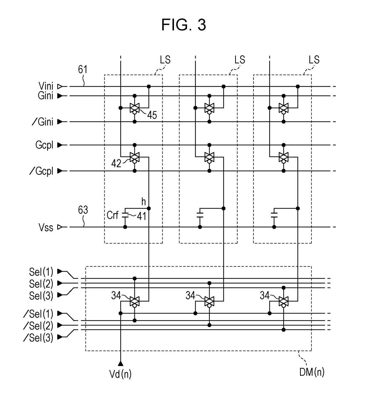
[0140]In the embodiments described above, the third transistor 123 is coupled between a drain of the drive transistor 121 and the second data transfer line 14-2, in each pixel circuit 110, but the third transistor 123 may be coupled between the drain and the gate g of the drive transistor 121, as illustrated in FIG. 13.
modification example 2
[0141]In each pixel circuit 110 in the embodiments described above, the fifth transistor 125 may not be provided.
modification example 3
[0142]It is not necessary for the first transistor 126 described above to be disposed outside the pixel circuit 110, and the first transistor 126 may be disposed inside each pixel circuit 110.
Login to View More PUM
 Abstract
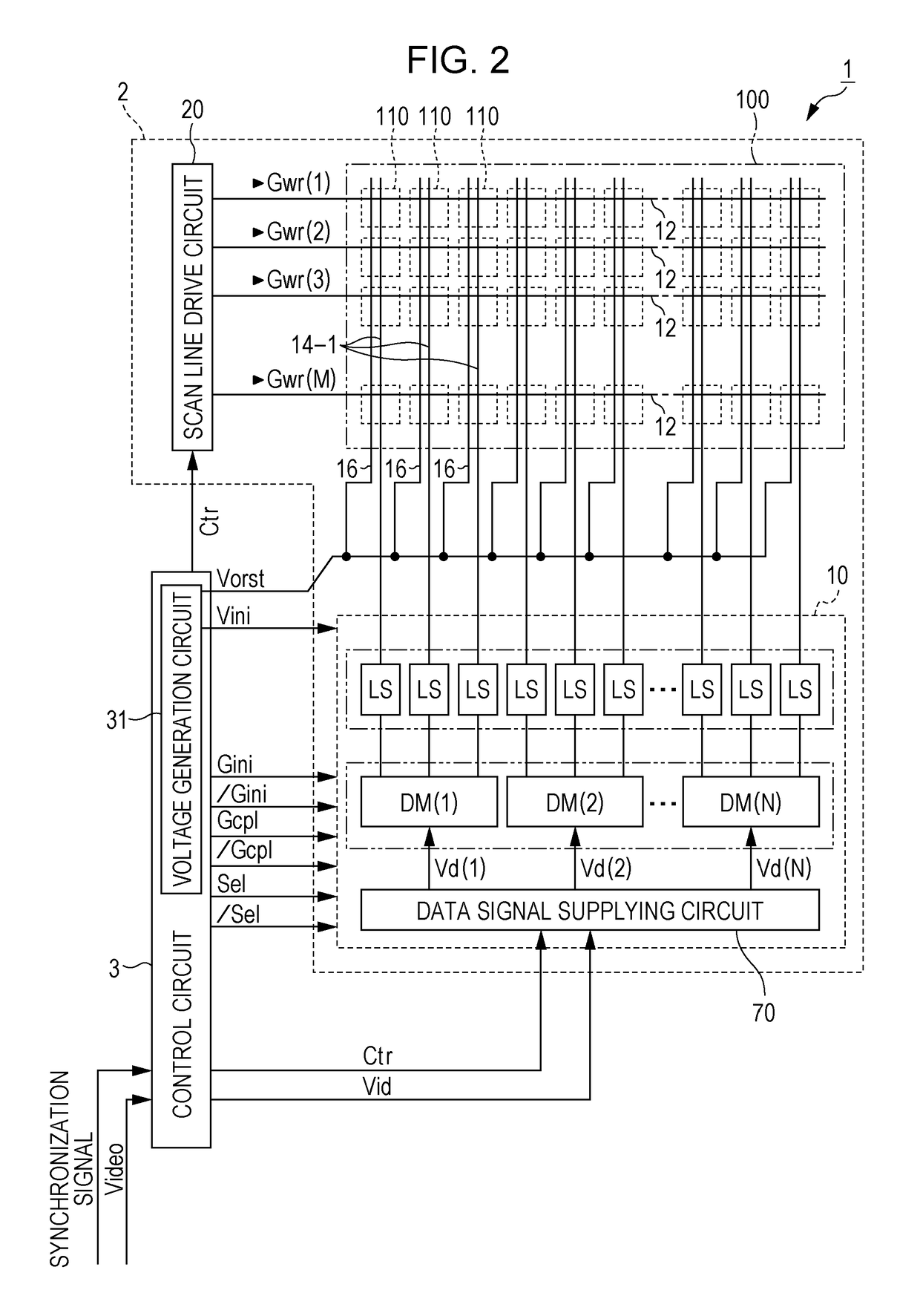
An electro-optical device includes a first data transfer line that intersects a scan line, a second data transfer line, a first transistor that controls coupling between the first data transfer line and the second transfer line. The two or more second data transfer lines are respectively coupled to the first data transfer line via first capacitors, and when a collection of pixel circuits that are coupled to the same first data transfer line via the second data transfer lines is referred to as a pixel string, the second data transfer lines are provided to pixel circuits less than the pixel circuits included in the pixel string.
Description
BACKGROUND[0001]1. Technical Field[0002]The present invention relates to an electro-optical device, an electronic apparatus, and a method of driving the electro-optical device.[0003]2. Related Art[0004]In recent years, various electro-optical devices that use a light emitting element such as an organic light emitting diode (hereinafter, referred to as OLED) have been proposed. In a general configuration of the electro-optical device, an image circuit that includes a light emitting element, a transistor, or the like is provided in correspondence with pixels of an image to be displayed, corresponding to intersection of scan lines and data lines.[0005]In the configuration, if a data signal of a potential according to a gradation level of pixels is applied to a gate of the transistor, the transistor supplies a light emitting element with a current according to a gate-source voltage. According to this, the light emitting element emits light in brightness according to a gradation level.[0...
Claims
Login to View More Application Information
Patent Timeline
 Patent Type & AuthorityPatents(United States)
IPC IPC(8): G09G3/3233G09G3/00G09G3/3291H05B44/00
CPCG09G3/3233G09G3/003G09G3/3291G09G2300/0819G09G2320/045G09G2300/0861G09G2310/0251G09G2320/043G09G2300/0842
InventorOTA, HITOSHIKOSHIHARA, TAKESHI
OwnerSEIKO EPSON CORP