Touch sensor

a capacitive touch and sensor technology, applied in the field of position-sensitive capacitive touch sensors, to achieve the effect of improving noise performan

Active Publication Date: 2019-03-19
SOLOMON SYSTECH
View PDF10 Cites 1 Cited by
  • Summary
  • Abstract
  • Description
  • Claims
  • Application Information

AI Technical Summary

Benefits of technology

[0060]By co-extending, interdigitating or interleaving multiple higher order branches of the X and Y electrodes, it is possible to produce a more uniform electrical field distribution across the sub-area associated with each node (i.e. there are no dead spots such as present in the diamond pattern design). The magnitude of perturbances of touches to the electrical field become a monotonal, i.e. single valued, function of surface area of the touch, thereby simplifying the post-processing which is performed to determine touch location and size.
[0061]By co-extending, interdigitating or interleaving multiple higher order branches of the X and Y electrodes can also deliver significant benefits for the edges, since the sensitivity and linearity can be maintained right up to the edge of the touch sensitive area, i.e. in the nodes that are at the edge of the node array, allowing bezel free touch screen devices to be realized with substantially linear touch sensitivity right up to the edges.
[0062]By co-extending, interdigitating or interleaving multiple higher order branches of the X and Y electrodes, it is possible to make the electrode pattern such that the X and Y nodes are coincident with each other (not offset as in a diamond pattern for example). In particular the X and Y nodes can be arranged to form an array of square nodal areas. This enables the perturbances of a touch to X and Y electric fields to be considered independently in each of the X and Y axes (i.e. avoiding the coupling of X and Y axis perturbances that occurs in a diamond pattern for example). This further simplifies the post-processing performed by position finding algorithms, thereby improving linearity, accuracy and speed of touch determination. Moreover, for self capacitance measurements, when the touch size is smaller than the node area, there is always positional information in both X and Y axes (unlike a diamond pattern which has blind spots where touch location information in one axis is missing for small area touches on axis). Still further, making the X and Y nodes coincident with each other means that the signals associated with mutual capacitance and self capacitance measurements are centered at the same location (unlike a diamond pattern where self capacitance signal is centered in the middle of the diamonds and mutual capacitance signal is concentrated at the gaps between X and Y diamonds).
[0065]Co-extending, interdigitating or interleaving of X and Y higher order branches also allows electrode patterns which provide shielding of the Y electrodes (e.g. sense electrodes in mutual capacitance) by the X electrodes (e.g. drive electrodes in mutual capacitance), thereby to improve noise performance.
[0066]In the following we describe in more detail various designs of capacitive touch sensor device comprising set of crossing X and Y electrodes whose crossing points form a two-dimensional array of nodes which define a touch sensitive area. In these designs, by varying the dimensions of the electrode branches, such as width and length, and the gaps between them, the overall area of the X and Y electrodes can be varied relatively independently of each other. It is therefore possible to produce an electrode pattern in which the self capacitances of the X and Y electrodes have a certain ratio, e.g. unity, and thereby compensate for the aspect ratio of the touch sensitive area, and / or to have a certain absolute value, e.g. in order not to overload a touch-sensor controller to which the sensor is to be connected.

Problems solved by technology

However, there is a trade off, since these pinch points form the largest resistance elements, and thereby can become the rate limiting factor for charge times. Away from the XY crossing points, it is beneficial for the electrodes to spread out to more or less cover the whole panel sub-area associated with the node.

Method used


Image

  • Touch sensor
  • Touch sensor
  • Touch sensor

Examples


Embodiment Construction

[0105]In the following detailed description, for purposes of explanation and not limitation, specific details are set forth in order to provide a better understanding of the present disclosure. It will be apparent to one skilled in the art that the present disclosure may be practiced in other embodiments that depart from these specific details.

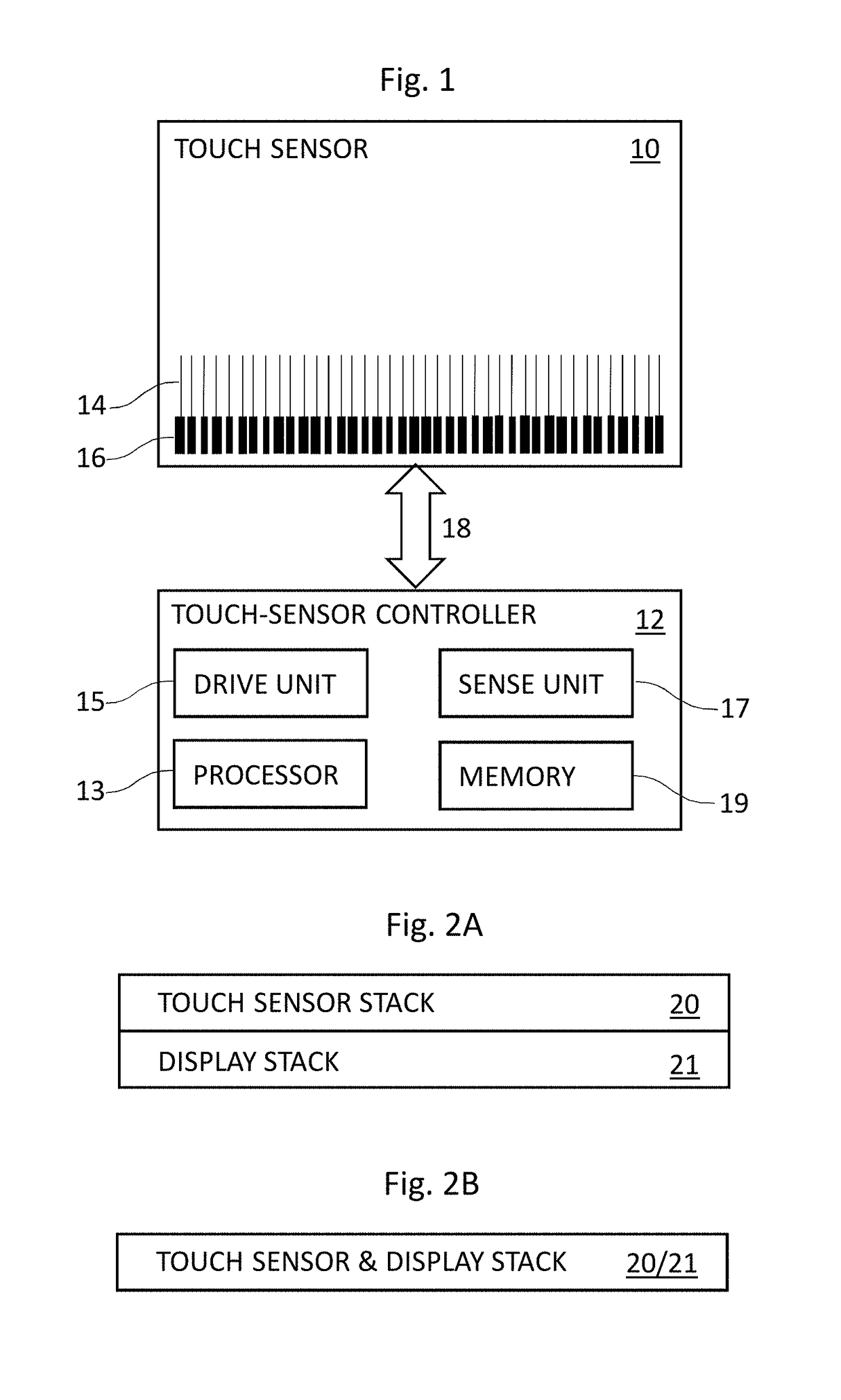
[0106]FIG. 1 illustrates an example touch sensor 10 with an example touch-sensor controller 12, often referred to in the art as a touch integrated circuit (touch IC) or touch sensor / screen controller / chip (TSC). The touch sensor 10 and the touch-sensor controller 12 may detect the presence and location of a touch or the proximity of an object within a touch-sensitive area of the touch sensor 10. The touch sensor 10 may include one or more touch-sensitive areas. The touch sensor 10 may include an array of electrodes which may be arranged in a single layer or multiple layers. The electrode array will usually be of a conductive material, each lay...


PUM


Abstract

A capacitive touch sensor device comprising set of crossing X and Y electrodes whose crossing points form a two-dimensional array of nodes which define a touch sensitive area. As well as the main electrode spines which cross, referred to as zeroth order electrode branches, the electrodes have higher order branches, some of which interdigitate. By varying the dimensions of the electrode branches, such as width and length, the overall area of the X and Y electrodes can be varied relatively independently of each other. It is therefore possible to produce an electrode pattern in which the self capacitances of the X and Y electrodes have a certain ratio, e.g. unity, and thereby compensate for the aspect ratio of the touch sensitive area, and / or to have a certain absolute value, e.g. in order not to overload a touch-sensor controller to which the sensor is to be connected.

Description

CROSS-REFERENCE TO THE RELATED APPLICATION[0001]This application claims priority to the United Kingdom Patent Application No. GB1702111.4, filed Feb. 9, 2017, the disclosure of which is incorporated herein by reference in their entirety.FIELD OF THE INVENTION[0002]The present disclosure relates to position-sensitive capacitive touch sensors, more especially, but not exclusively, to capacitive touch sensors integrated with displays to form touch screens.BACKGROUND[0003]A capacitive touch sensor, referred to simply as a touch sensor in the following, may detect the presence and location of a touch or the proximity of an object (such as a user's finger or a stylus) on a surface. Touch sensors are often combined with a display to produce a touch screen. In other devices, the touch sensors are not combined with a display, e.g. a touch pad of a laptop computer. A touch screen enables a user to interact directly with what is displayed on the screen through a graphical user interface (GUI),...

Claims


Application Information

Patent Timeline
Patent Type & Authority Patents(United States)
IPC IPC(8): G06F3/044G06F3/047G06F3/041
CPCG06F3/044G06F3/047G06F3/0416G06F2203/04112G06F2203/04103G06F3/0443G06F3/0446G06F3/0448G06F3/0412
Inventor CHURCH, JUSTIN ANTHONYGUARD, DAVID BRENT
Owner SOLOMON SYSTECH
Why Eureka
Try Eureka