
Rectangular chip resistor and manufacturing method for same

a technology of resistor and chip, which is applied in the direction of resistor chip manufacture, resistor details, resistor manufacturing, etc., can solve the problems of small region of the divided resistive element that may have risk of current load constriction, difficulty in sufficiently suppressing current turbulence, and difficulty in precisely setting resistance during the formation of trimming slots, etc., to achieve the effect of wide range of desired resistance, reduced current constriction, and improved tolerance to overload curren

Active Publication Date: 2019-03-26
KAMAYA ELECTRIC
View PDF21 Cites 5 Cited by
  • Summary
  • Abstract
  • Description
  • Claims
  • Application Information

AI Technical Summary

Benefits of technology

The present invention provides a rectangular chip resistor with improved resistance to current constriction and overload current. The resistor has a distinct division of the regions where the electrodes are in contact with the resistive element, and a trimming slot is formed in the non-contacting regions to ensure sufficient area for current flow. The direction of trimming slots is aligned with the current flow direction to suppress current constriction. The length and number of trimming slots and contacting regions of the resistive element can be controlled to achieve a wide range of desired resistance. The production method allows for precise control of resistance settings and a wider range of resistance adjustments, while suppressing microcracks and the effect of current overload.

Problems solved by technology

These prior art trimming slots, however, are formed linearly or in L-shape by first cutting out the slots at generally right angles to the direction of the current flowing through the resistive element, so that it is difficult to sufficiently suppress the current turbulence caused by the trimming slots.
In this case, since the resistive element is not reliably cut out from the electrodes due to the trimming slot, it is difficult to precisely set the resistance during the formation of the trimming slots.
In addition, the resistive element is completely divided by the trimming slot in the current-carrying condition, so that the smaller region of the divided resistive element may have risk of current load constriction.

Method used


Image

  • Rectangular chip resistor and manufacturing method for same
  • Rectangular chip resistor and manufacturing method for same
  • Rectangular chip resistor and manufacturing method for same

Examples


examples

[0081]The present invention will now be explained in further detail with reference to examples, which however, do not limit the present invention.

examples 1-1 to 1-3

[0082]Resistors as shown in FIG. 8 were produced using the first and second top electrodes and the resistive element having the trimming slots, as shown in FIG. 5, to have the rated power of 0.1 W, 0.25 W, 0.33 W, and 0.4 W, respectively. The insulating substrate was composed of a 96% alumina substrate; the top electrodes of silver-palladium-containing metal films; the bottom electrodes of silver-containing metal films; the resistive element of a resistive film using a ruthenium-oxide-containing special resistant material; the end electrodes of nickel-chromium-containing metal films formed by sputtering, the protective film 83a of a glass-type film; the protective film 83b of a silver-palladium-containing film; the plated layer 85 of a nickel plated layer; and the plated layer 86 of a tin plated layer, respectively.

[0083]In Example 1-1 the angle θ in FIG. 5 was 70°, in Example 1-2 the angle θ was 79°, and in Example 1-3 the angle θ was 87°.

[0084]The short time overload test was cond...


PUM


Abstract

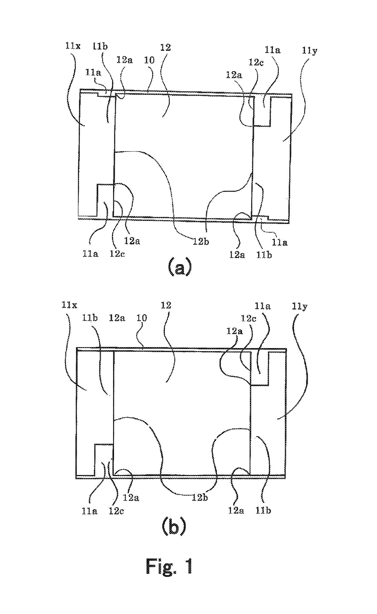
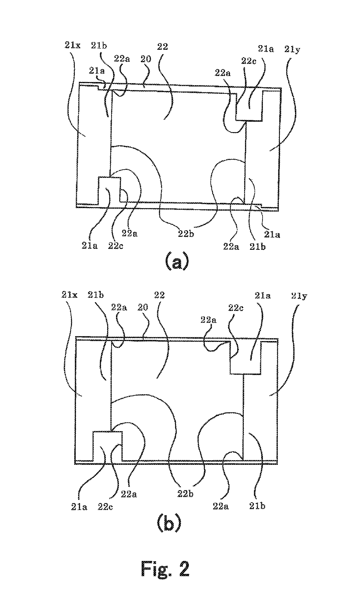
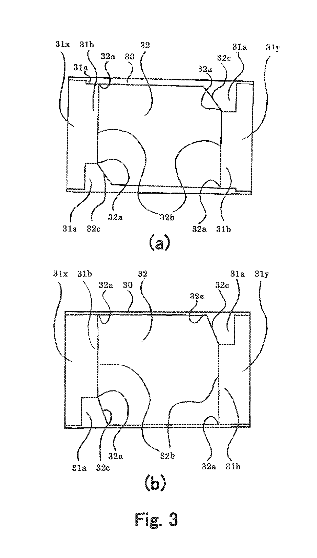
The chip resistor includes insulating substrate 10, first and second top electrodes (11x, 11b) on the top surface of the insulating substrate each on either longitudinal end thereof, and resistive element 12 electrically in contact with the top electrodes, wherein each of the top electrodes has, on its inner side facing to the other, cutout part 11a and protruding part 11b, with the cutout part in the first top electrode extending from at least one longitudinal side of the insulating substrate, transversely inwards thereof, and with the cutout part in the second top electrode arranged substantially point-symmetrically to the cutout part in the first top electrode with respect to the center of the insulating substrate, wherein the resistive element has contacting regions 12b, and non-contacting regions 12c, and trimming slot (53a, 53b) including a linear part.

Description

[0001]This is the national stage of International Application PCT / JP2016 / 062724, filed Apr. 22, 2016.FIELD OF ART[0002]The present invention relates to a rectangular chip resistor and a method for producing the same, in which current constriction caused by trimming slots that have been formed for adjustment of resistance, is suppressed, and which has excellent tolerance to overload, such as surge current.BACKGROUND ART[0003]For adjusting resistance of a chip resistor, there is widely known to form trimming slots in its resistive element. There are conventionally known, for example as shown in FIGS. 9(A) and 9(B), trimming slots 93a formed as linear cuts at generally right angles to the direction of the current flowing through a resistive element 92 from a pair of top electrodes 91 disposed on the top surface of an insulating substrate 90 on both ends, and a trimming slot 93b formed as an L-shaped cut. Disadvantageously, the flow of the current 94 is turbulent at the tip or at the L-...

Claims


Application Information

Patent Timeline
Patent Type & Authority Patents(United States)
IPC IPC(8): H01C13/02H01C7/00H01C17/06H01C17/00H01C17/065H01C1/142H01C17/242
CPCH01C13/02H01C1/142H01C7/003H01C17/242H01C17/06H01C17/065H01C17/006H01C7/00
Inventor MORITA, TOMIHARUNOJIRI, YUUSUKE
Owner KAMAYA ELECTRIC
Learn More