Semiconductor device

a technology of semiconductors and devices, applied in the direction of semiconductor devices, basic electric elements, electrical equipment, etc., can solve the problems of leak current generation and parasitic capacitance generated by electrode wiring, and achieve the effect of suppressing parasitic capacitance and leak current in gate wires, improving pinch-off characteristics of transistors, and improving parasitic capacitance and leak curren

Active Publication Date: 2015-06-25
PANASONIC INTELLECTUAL PROPERTY MANAGEMENT CO LTD
View PDF7 Cites 14 Cited by
  • Summary
  • Abstract
  • Description
  • Claims
  • Application Information

AI Technical Summary

Benefits of technology

[0036]According to the nitride semiconductor according to the present invention, a parasitic capacitance and a leak current in a gate wire can be suppressed while pinch-off characteristics of a transistor are improved.

Problems solved by technology

The nitride semiconductor device described in Patent Literature 1 includes a conductive nitride semiconductor layer immediately below electrode wiring, and therefore has the following problem: a parasitic capacitance associated with electrode wiring is generated, and a leak current is generated between a source electrode and a drain electrode, and a gate electrode.

Method used


Image

  • Semiconductor device
  • Semiconductor device
  • Semiconductor device

Examples


first exemplary embodiment

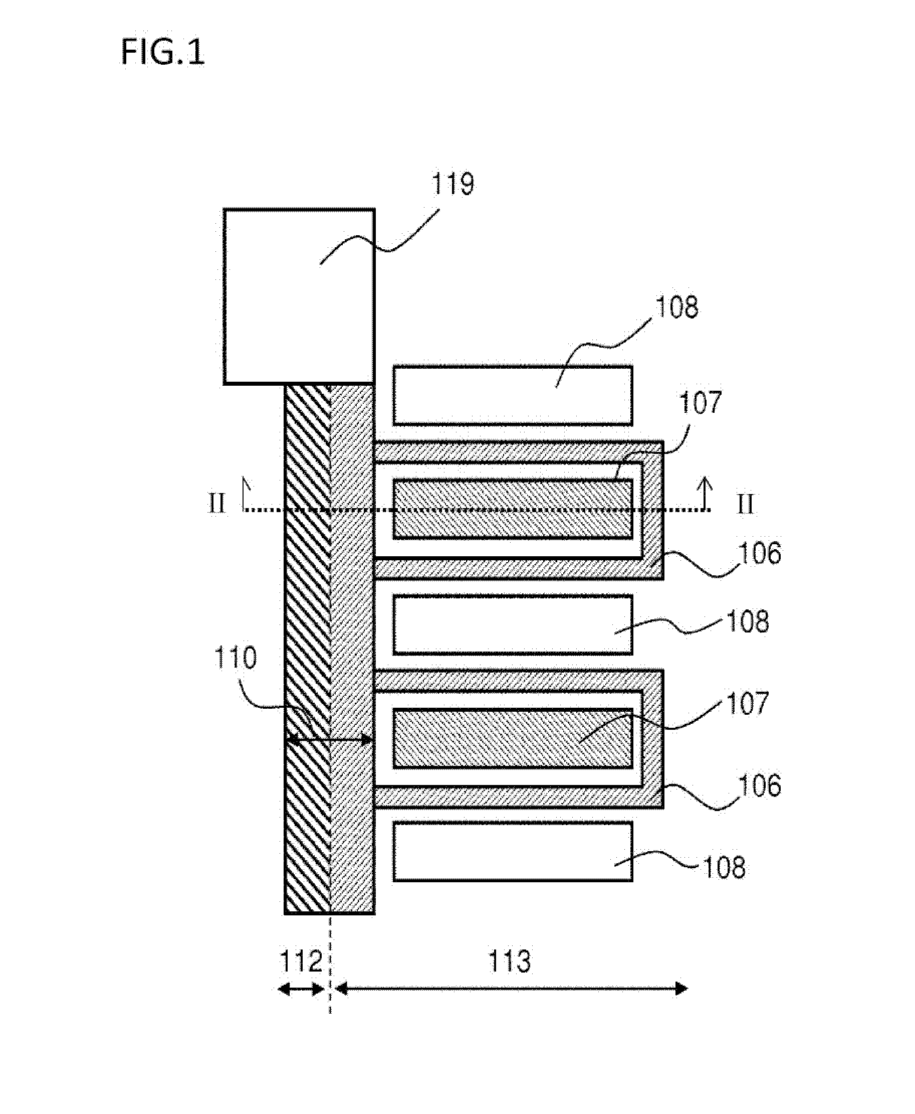
[0070]FIG. 1 is a plan view showing a structure of a semiconductor device including a nitride semiconductor, i.e., a nitride semiconductor device according to a first exemplary embodiment of the present invention.

example 1-1

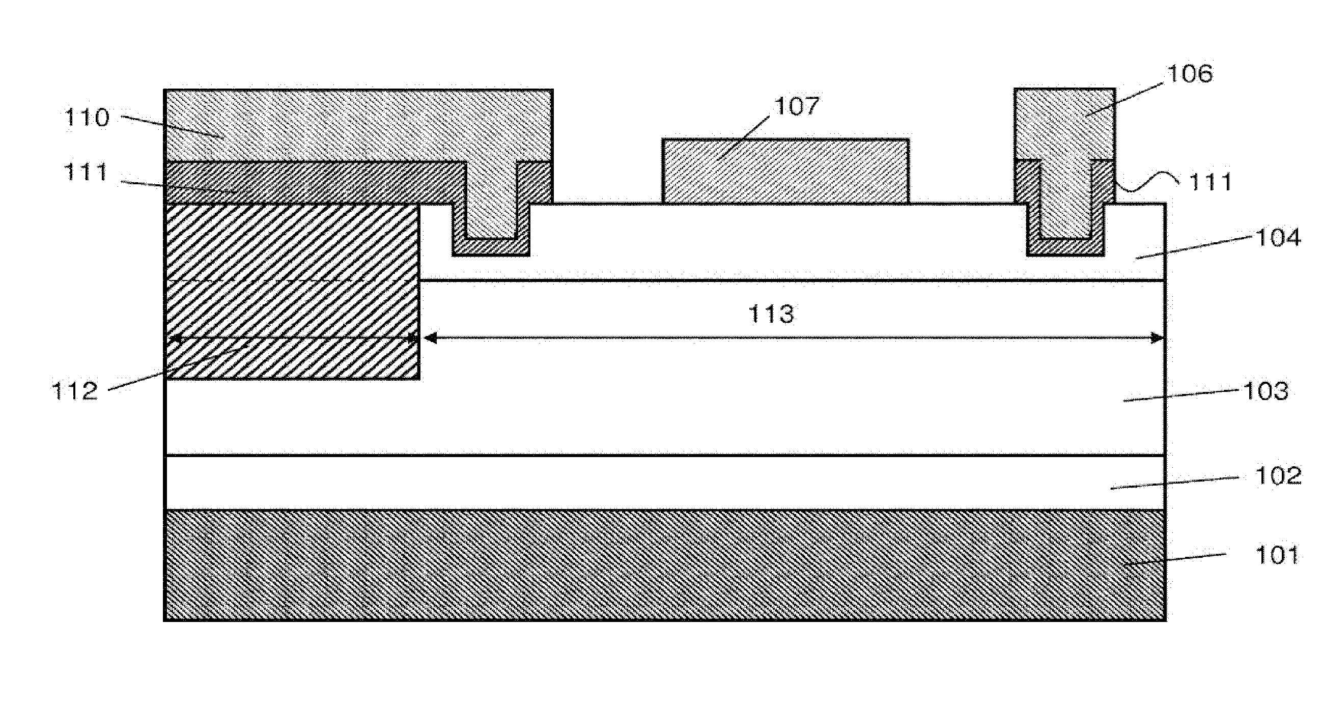
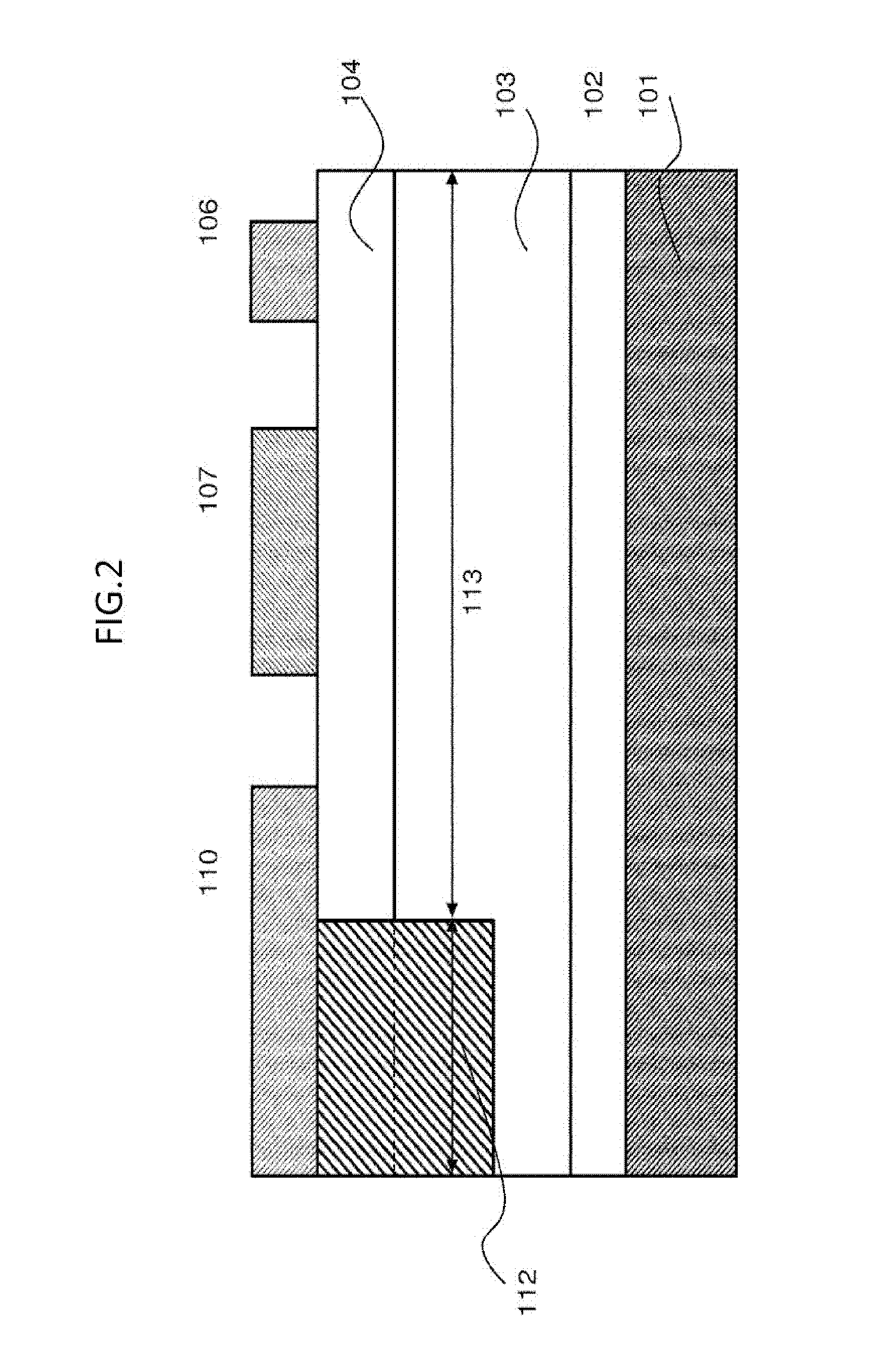
[0071]FIG. 2 is a sectional view showing a structure of the nitride semiconductor device along dashed line II-II shown in FIG. 1. In the present application, hatching is appropriately omitted in the sectional view for avoiding complication.

[0072]The nitride semiconductor device according to Example 1 of the present exemplary embodiment is configured such that, for example, 100 nm-thick buffer layer 102 made of AlN, 2 μm-thick undoped GaN layer 103, and 20 nm-thick undoped AlGaN layer 101 having an Al composition ratio of 20% are epitaxially grown in this order on, for example, 600 μm-thick substrate 101 made of silicon, and for example, source electrode 107 having a laminated structure of Ti and Al and drain electrode 108 having a laminated structure of Ti and Al are formed so as to be in ohmic contact with undoped AlGaN layer 104. For example, gate electrode 106 made of Ni and gate wire 110 made of Au are formed so as to be in Schottky contact with undoped AlGaN layer 104. Gate wir...

example 1-2

[0089]A nitride semiconductor device according to Example 2 of the present invention is the same as that according to Example 1 for the plan view of FIG. 1, and as shown in FIG. 5, the nitride semiconductor device is different from that according to Example 1 only in a cross section structure along dashed line II-II shown in FIG. 1.

[0090]As shown in FIG. 5, the nitride semiconductor device according to the present example is configured such that p-type semiconductor layer 105 is formed on undoped AlGaN layer 104, and gate electrode 106 and gate wire 110 are formed so as to be in contact with p-type semiconductor layer 105. As p-type semiconductor layer 105, a Mg-doped p-type GaN layer having a layer thickness of 200 nm is used. Here, gate electrode 106 and gate wire 110 may be in Ohmic contact with p-type semiconductor layer 105, or may be in Schottky contact with p-type semiconductor layer 105. For gate electrode 106 that is in ohmic contact with the p-type semiconductor layer, for...


PUM


Abstract

A parasitic capacitance and a leak current in a nitride semiconductor device are reduced. For example, a 100 nm-thick buffer layer made of AlN, a 2 μm-thick undoped GaN layer, and 20 nm-thick undoped AlGaN having an Al composition ratio of 20% are epitaxially grown in this order on, for example, a substrate made of silicon, and a source electrode and a drain electrode are formed so as to be in ohmic contact with the undoped AlGaN layer. Further, in the undoped GaN layer and the undoped AlGaN layer immediately below a gate wire, a high resistance region, the resistance of which is increased by for example, ion implantation with Ar or the like, is formed, and a boundary between the high resistance region and an element region is positioned immediately below the gate wire.

Description

TECHNICAL FIELD[0001]The present invention relates to a semiconductor device including a nitride semiconductor, which can be applied to a power switching element that is used in, for example, a power supply circuit of consumer equipment.BACKGROUND ART[0002]Group III nitride semiconductors typified by gallium nitride (GaN) are wide-gap semiconductors. For example, the forbidden band gaps of gallium nitride (GaN) and aluminum nitride (AlN) are as large as 3.4 eV and 6.2 eV, respectively, at room temperature. Such nitride semiconductors are characterized by having a large breakdown electric field and a higher electron saturation speed than a compound semiconductor such as gallium arsenide (GaAs), silicon (Si), and the like. Then, field effect transistors (FET) using a GaN-based compound semiconductor material have been actively researched and developed as high frequency electronic devices or high power electronic devices.[0003]A nitride semiconductor material such as GaN forms various ...

Claims


Application Information

Patent Timeline
Patent Type & Authority Applications(United States)
IPC IPC(8): H01L29/10H01L29/06H01L29/20H01L29/78
CPCH01L29/1083H01L29/2003H01L29/0661H01L29/78H01L29/42316H01L29/4238H01L29/7786H01L29/41758H01L29/1066H01L29/4236H01L29/10H01L29/06H01L29/20
Inventor UMEDA, HIDEKAZUKAIBARA, KAZUHIROTAMURA, SATOSHI
Owner PANASONIC INTELLECTUAL PROPERTY MANAGEMENT CO LTD
Why Eureka
Try Eureka