Semiconductor device, method for manufacturing the same, or display device including the same

a semiconductor and film technology, applied in semiconductor devices, instruments, computing, etc., can solve problems such as adversely affecting transistor characteristics, and achieve the effects of reducing wiring resistance, increasing transistor mobility, and increasing the integration degree of an integrated circui

Active Publication Date: 2019-04-16
SEMICON ENERGY LAB CO LTD
View PDF199 Cites 1 Cited by
  • Summary
  • Abstract
  • Description
  • Claims
  • Application Information

AI Technical Summary

Benefits of technology

[0008]Reducing the resistance of a wiring, as well as increasing the mobility of a transistor, is effective in increasing the integration degree of an integrated circuit and miniaturizing an image display device. As a material for a wiring in a semiconductor device, copper has been examined. In the case of using a copper wiring, a barrier layer that prevents copper in the copper wiring from diffusing into a semiconductor film is required in order not to impair the transistor characteristics. The barrier layer can also prevent diffusion of impurities into the copper wiring and a reduction in the conductivity of the copper wiring.
[0010]Furthermore, in the case where a carrier supply source is generated near a source and a drain in a channel formed of an oxide semiconductor film, effective channel lengths are shortened or varied. The carrier supply source is formed with oxygen vacancy and hydrogen; therefore, it is particularly necessary to prevent oxygen diffusion from the oxide semiconductor film to the source and the drain.
[0011]In view of the foregoing problems, an object of one embodiment of the present invention is to suppress a change in electrical characteristics and to improve reliability in a transistor including an oxide semiconductor film. Another object of one embodiment of the present invention is to provide a semiconductor device with low power consumption. Another object of one embodiment of the present invention is to provide a novel semiconductor device. Another object of one embodiment of the present invention is to provide a novel display device.
[0018]In a transistor including an oxide semiconductor film of one embodiment of the present invention, a change in electrical characteristics can be suppressed and reliability can be improved. According to one embodiment of the present invention, a novel semiconductor device can be provided. According to one embodiment of the present invention, a novel display device can be provided.

Problems solved by technology

In a transistor using an oxide semiconductor film for a channel region, oxygen vacancy which is formed in the oxide semiconductor film adversely affects the transistor characteristics.

Method used


Image

  • Semiconductor device, method for manufacturing the same, or display device including the same
  • Semiconductor device, method for manufacturing the same, or display device including the same
  • Semiconductor device, method for manufacturing the same, or display device including the same

Examples


embodiment 1

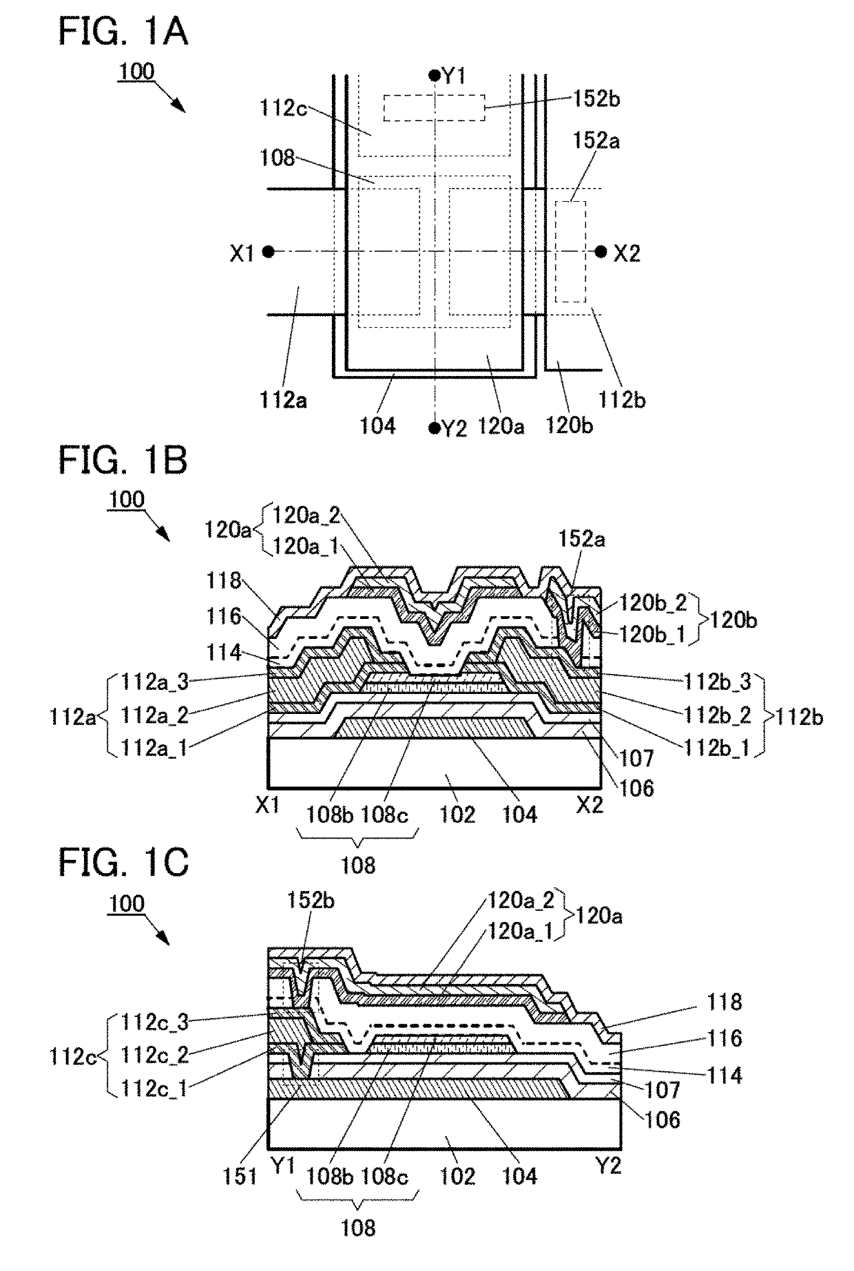
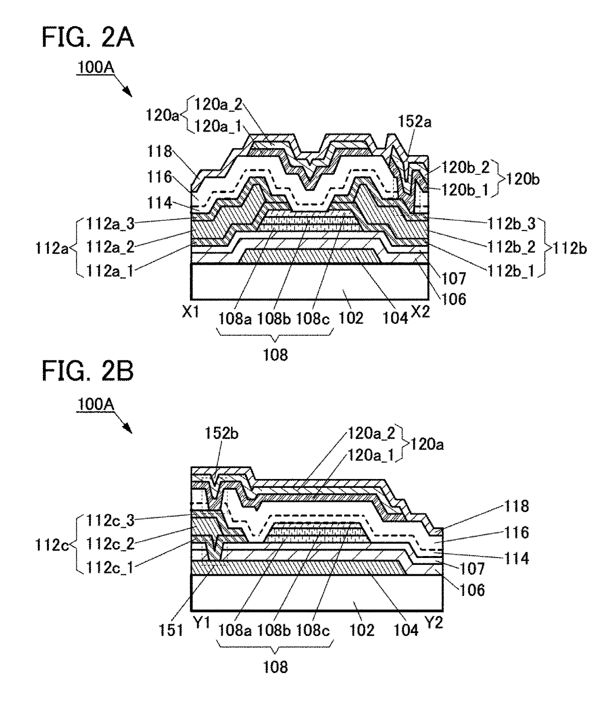
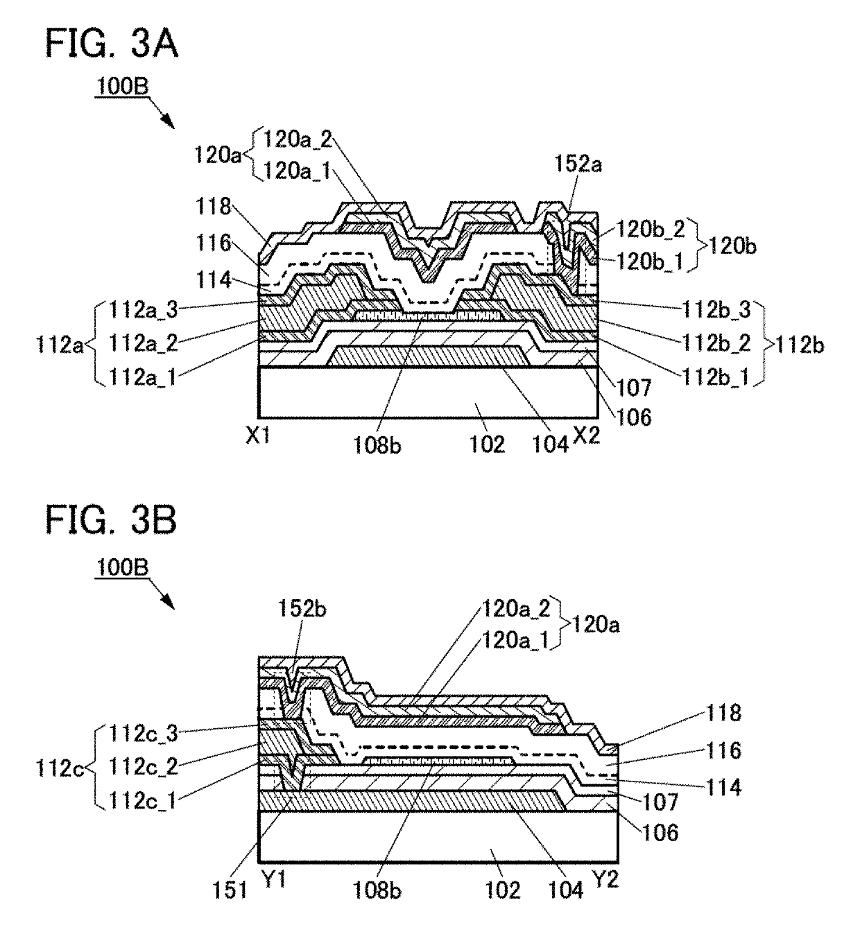
[0090]In this embodiment, a semiconductor device of one embodiment of the present invention and a manufacturing method thereof are described with reference to FIG. 1A to FIG. 12.

[0091]FIG. 1A is a top view of a transistor 100 that is a semiconductor device of one embodiment of the present invention. FIG. 1B is a cross-sectional view taken along a dashed-dotted line X1-X2 in FIG. 1A, and FIG. 1C is a cross-sectional view taken along a dashed-dotted line Y1-Y2 in FIG. 1A. Note that in FIG. 1A, some components of the transistor 100 (e.g., an insulating film serving as a gate insulating film) are not illustrated to avoid complexity. The direction of the dashed-dotted line X1-X2 may be called a channel length direction, and the direction of the dashed-dotted line Y1-Y2 may be called a channel width direction. As in FIG. 1A, some components are not illustrated in some cases in top views of transistors described below.

[0092]The transistor 100 includes a conductive film 104 over a substrate...

embodiment 2

[0259]In this embodiment, the composition, the structure, and the like of an oxide semiconductor that can be used in one embodiment of the present invention are described with reference to FIGS. 13A to 13C, FIG. 14, FIGS. 15A and 15B, FIGS. 16A to 16E, FIGS. 17A to 17E, FIGS. 18A to 18D, FIGS. 19A and 19B, and FIG. 20.

[0260]Composition of an oxide semiconductor is described below. Note that in this embodiment, an oxide semiconductor is also simply referred to as an oxide to describe its composition.

[0261]An oxide preferably contains at least indium or zinc. In particular, indium and zinc are preferably contained. In addition, aluminum, gallium, yttrium, tin, or the like is preferably contained. Furthermore, one or more elements selected from boron, silicon, titanium, iron, nickel, germanium, zirconium, molybdenum, lanthanum, cerium, neodymium, hafnium, tantalum, tungsten, magnesium, or the like may be contained.

[0262]Here, the case where an oxide contains indium, an element M, and z...

embodiment 3

[0344]In this embodiment, an example of a display device that includes the transistor described in the above embodiments is described below with reference to FIG. 21 to FIG. 27.

[0345]FIG. 21 is a top view illustrating an example of a display device. A display device 700 in FIG. 21 includes a pixel portion 702 provided over a first substrate 701, a source driver circuit portion 704 and a gate driver circuit portion 706 that are provided over the first substrate 701, a sealant 712 provided to surround the pixel portion 702, the source driver circuit portion 704, and the gate driver circuit portion 706, and a second substrate 705 provided to face the first substrate 701. The first substrate 701 and the second substrate 705 are sealed with the sealant 712. That is, the pixel portion 702, the source driver circuit portion 704, and the gate driver circuit portion 706 are enclosed by the first substrate 701, the sealant 712, and the second substrate 705. Although not illustrated in FIG. 21...


PUM


Abstract

A gate electrode, a first insulating film thereover, an oxide semiconductor film thereover, a source electrode and a drain electrode thereover, and a second insulating film thereover are included. The source and the drain electrodes each include a first conductive film, a second conductive film over and in contact with the first conductive film, and a third conductive film over and in contact with the second conductive film. The second conductive film includes copper. The first and the third conductive films each include an oxide conductive film. An end portion of the first conductive film includes a region located outward from an end portion of the second conductive film. The third conductive film covers a top surface and a side surface of the second conductive film and includes a region in contact with the first conductive film.

Description

BACKGROUND OF THE INVENTION[0001]1. Field of the Invention[0002]One embodiment of the present invention relates to a semiconductor device including an oxide semiconductor film and a display device including the semiconductor device. Another embodiment of the present invention relates to a manufacturing method of the semiconductor device including an oxide semiconductor film.[0003]Note that one embodiment of the present invention is not limited to the above technical field. The technical field of one embodiment of the invention disclosed in this specification and the like relates to an object, a method, or a manufacturing method. In addition, one embodiment of the present invention relates to a process, a machine, manufacture, and a composition of matter. In particular, one embodiment of the present invention relates to a semiconductor device, a display device, a light-emitting device, a power storage device, a storage device, a driving method thereof, and a manufacturing method ther...

Claims


Application Information

Patent Timeline
Patent Type & Authority Patents(United States)
IPC IPC(8): H01L29/04H01L29/786H01L27/12H01L29/24H01L27/32G06F3/041
CPCH01L29/78606H01L27/1225H01L27/1255H01L29/045H01L29/7869H01L29/78696H01L29/24H01L27/3262G06F3/041H01L29/41733H01L29/42384H01L29/45H01L29/78642H10K59/1213
Inventor NAKAZAWA, YASUTAKAKOEZUKA, JUNICHI
Owner SEMICON ENERGY LAB CO LTD
Why Eureka
Try Eureka