Photo sensor circuit, photo sensor pixel, and display device having the photo sensor pixel

a photo sensor and circuit technology, applied in the field of electronic devices, can solve the problems of reducing the aperture ratio and resolution of the display panel, high panel defect rate, etc., and achieve the effects of simple structure, reduced area of the photo sensor circuit, and high sensitivity of photo sensing

Active Publication Date: 2019-04-30
SAMSUNG DISPLAY CO LTD
View PDF9 Cites 1 Cited by
  • Summary
  • Abstract
  • Description
  • Claims
  • Application Information

AI Technical Summary

Benefits of technology

[0005]In an in-cell type display panel, the addition of a touch sensor circuit and a photo sensor circuit increases the degree of circuit integration in the display panel, which results in a high panel defect rate. Also, the increase of the degree of circuit integration causes the aperture ratio and resolution of the display panel to decrease.
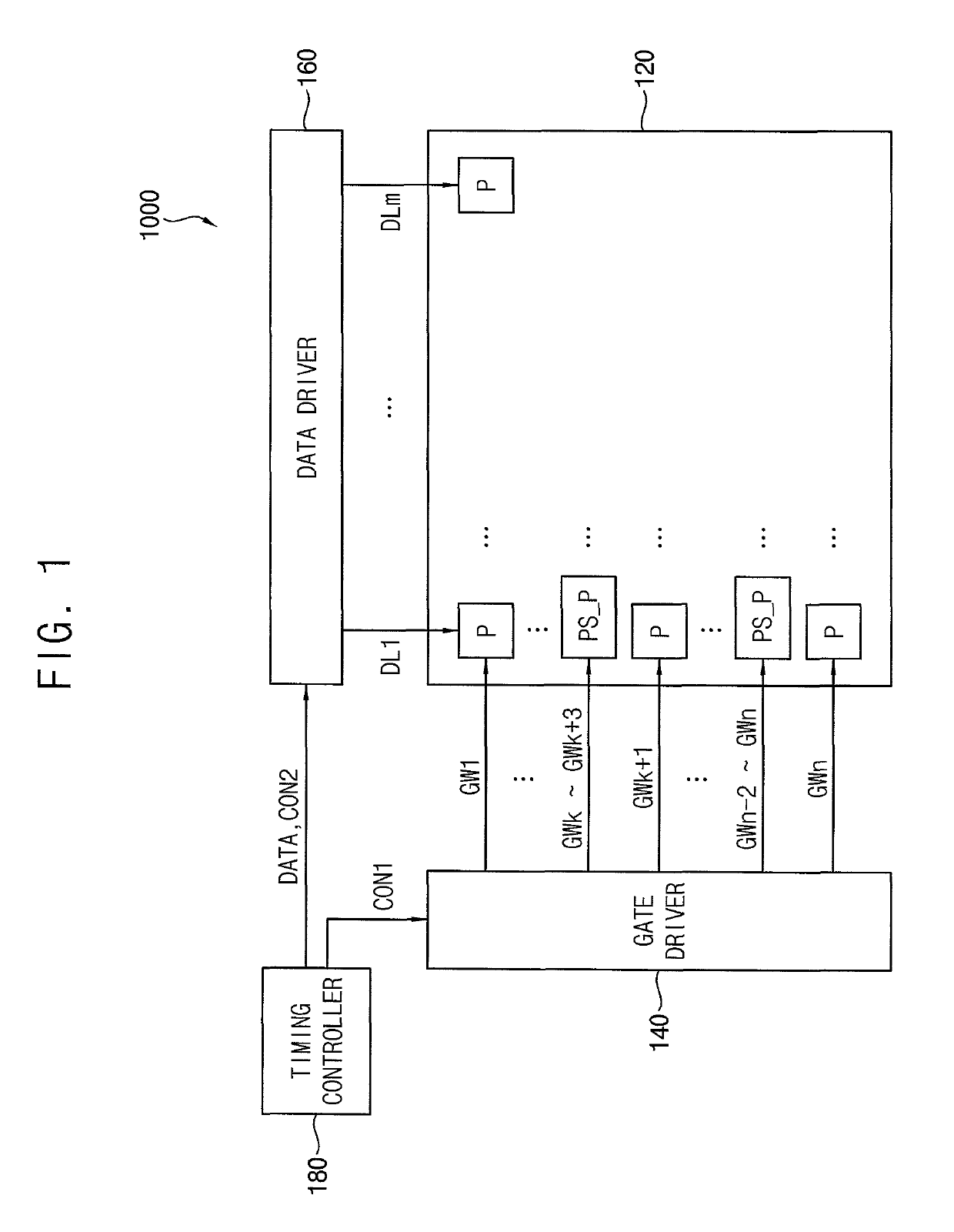
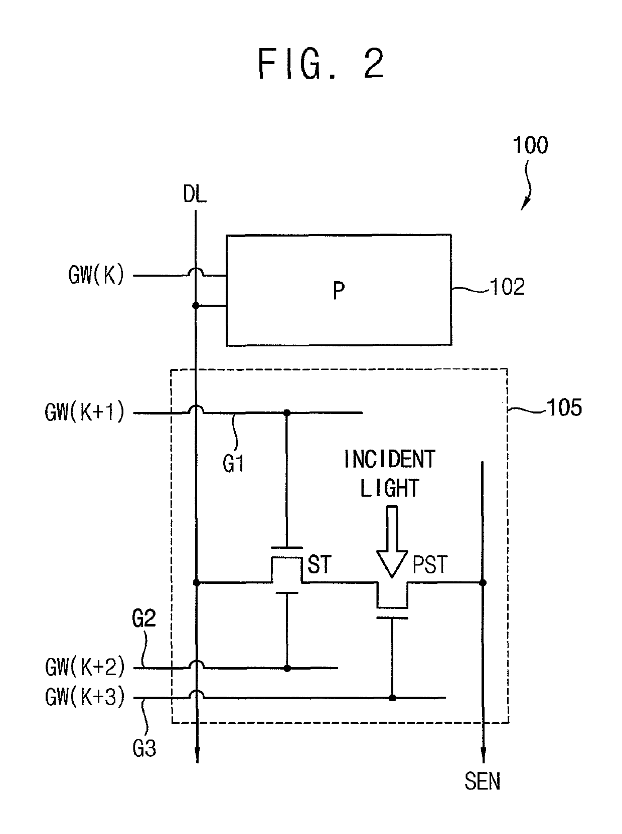
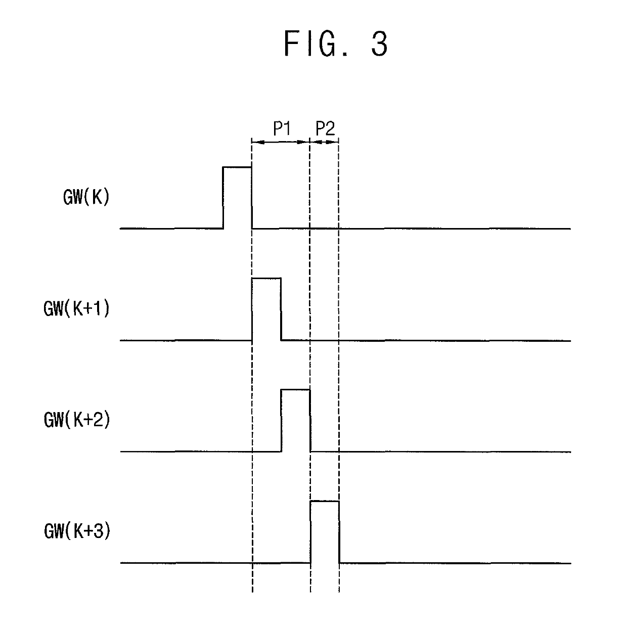
[0029]In such an embodiment, the photo sensor pixel may have a simple structure only including the switching transistor and the photo sensing transistor, so that the area of the photo sensor circuit may be reduced. In such an embodiment, since the switching transistor may be turned on by the plurality of gate signals, a high sensitivity of photo sensing may be ensured and the proportion of the photo sensor pixels occupied by the photo sensing display panel may be reduced.
[0030]In such an embodiment, the display device may include the photo sensing display panel having the in-cell type photo sensor pixels, so that the proportion of the photo sensor pixels occupied by the photo sensing display panel may be reduced. Thus, the photo sensing display panel such as the touch recognition, the fingerprint recognition, and the vein recognition can be realized while maintaining the sufficient aperture ratio and resolution without increasing a degree of circuit integration inside the photo sensing display panel.
[0031]In such an embodiment, the photo sensor pixel and the photo sensing display panel of the in-cell type may be realized without additional process and extra manufacturing cost for forming photo sensor circuits.

Problems solved by technology

In an in-cell type display panel, the addition of a touch sensor circuit and a photo sensor circuit increases the degree of circuit integration in the display panel, which results in a high panel defect rate.
Also, the increase of the degree of circuit integration causes the aperture ratio and resolution of the display panel to decrease.

Method used


Image

  • Photo sensor circuit, photo sensor pixel, and display device having the photo sensor pixel
  • Photo sensor circuit, photo sensor pixel, and display device having the photo sensor pixel
  • Photo sensor circuit, photo sensor pixel, and display device having the photo sensor pixel

Examples


Embodiment Construction

[0042]The invention now will be described more fully hereinafter with reference to the accompanying drawings, in which various embodiments are shown. This invention may, however, be embodied in many different forms, and should not be construed as limited to the embodiments set forth herein. Rather, these embodiments are provided so that this disclosure will be thorough and complete, and will fully convey the scope of the invention to those skilled in the art. Like reference numerals refer to like elements throughout.

[0043]It will be understood that when an element is referred to as being “on” another element, it can be directly on the other element or intervening elements may be therebetween. In contrast, when an element is referred to as being “directly on” another element, there are no intervening elements present.

[0044]It will be understood that, although the terms “first,”“second,”“third” etc. may be used herein to describe various elements, components, regions, layers and / or se...


PUM


Abstract

A photo sensor pixel includes a pixel circuit including a driving transistor, a switching transistor having a double gate structure and a photo sensing transistor connected in series with the switching transistor. The pixel circuit drives a light emitting element therein based on a data voltage provided thereto through a data line, the switching transistor includes a top gate electrode and a bottom gate electrode, which are connected to different gate lines, respectively, and the photo sensing transistor senses incident light.

Description

[0001]This application claims priority to Korean Patent Application No. 10-2017-0007295, filed on Jan. 16, 2017, and all the benefits accruing therefrom under 35 U.S.C. § 119, the content of which in its entirety is herein incorporated by reference.BACKGROUND1. Field[0002]Exemplary embodiments of the invention relate to an electronic device. More particularly, exemplary embodiments of the invention relate to a photo sensor circuit, a photo sensor pixel, and a display device including the same.2. Discussion of Related Art[0003]A display device includes a display panel for performing image display and a touch panel for recognizing a touch when a user's finger or a pen touches a specific position of a screen. The touch recognition method of the touch panel includes various types such as a pressure resistive type, an electrostatic capacity by contact type, a surface acoustic wave (“SAW”) type, an infrared light sensing type, and a piezoelectric type, or the like.[0004]In-cell type displ...

Claims


Application Information

Patent Timeline
Patent Type & Authority Patents(United States)
IPC IPC(8): G06F3/042G06F3/041H01L27/144
CPCG06F3/042G06F3/0412H01L27/1443H01L31/10
Inventor KIM, KEUNWOOPARK, SOOYOUNGPARK, JOONGHYUN
Owner SAMSUNG DISPLAY CO LTD
Why Eureka
Try Eureka