Touch panel, manufacturing method thereof, display device, and electronic apparatus

Active Publication Date: 2019-05-07
JAPAN DISPLAY INC
View PDF21 Cites 0 Cited by
  • Summary
  • Abstract
  • Description
  • Claims
  • Application Information

AI Technical Summary

Benefits of technology

[0012]In the touch panel, the manufacturing method thereof, the display device, and the electronic apparatus according to the embodiments of the present technology, a plurality of signal wires are hidden by two light blocking layers (the first light blocking layer and the second light blocking layer) which partially overlap each other. Here, the first light blocking layer is disposed relatively closer to the central region of the touch panel than the second light blocking layer and is provided in the wire substrate. For this reason, even if a joining error occurs at a position of the second light blocking layer when the wire substrate and the cover substrate are joined to each other, the error only varies an overlapping extent of the first light blocking layer and the second light blocking layer and thus does not influence the clearance between the first light blocking layer and the sensor electrode or the coat margin of the signal wires by the first light blocking layer. In other words, i

Problems solved by technology

However, if the light blocking film is too narrowed, there is a problem in that the signal wires are viewed from the outside due to joining errors wh

Method used


Image

  • Touch panel, manufacturing method thereof, display device, and electronic apparatus
  • Touch panel, manufacturing method thereof, display device, and electronic apparatus
  • Touch panel, manufacturing method thereof, display device, and electronic apparatus

Examples


Example

First Modified Example

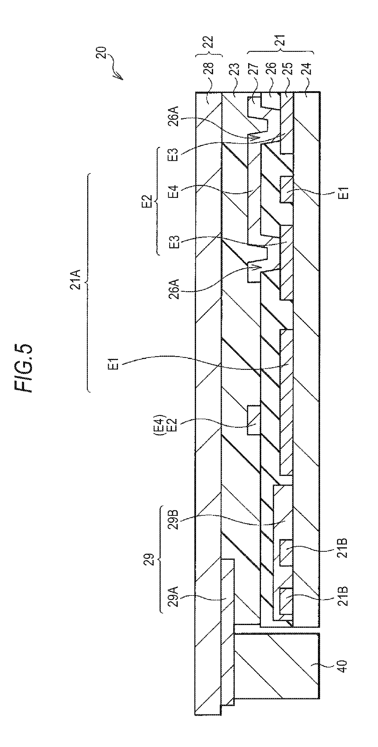
[0062]For example, although, in the above-described embodiment, the light blocking layer 29B covers all the signal wires 21B, the light blocking layer 29B may cover at least the signal wires 21B disposed closest to the sensor electrode 21A of a plurality of signal wires 21B. For example, as shown in FIGS. 12 and 13, the light blocking layer 29B may cover all the signal wires 21B excluding the signal wire 21B which is disposed so as to be the most distant from the sensor electrode 21A of the plurality of signal wires 21B. However, in the present modified example, it is necessary fora silhouette of the signal wire 21B which is not covered by the light blocking layer 29B not to be viewed from the outside. Specifically, it is at least necessary for the light blocking layer 29A to be disposed so as to face a continuous region including the outer edge region of the light blocking layer 29B and the signal wire 21B which is disposed so as to be the most distant from th...

Example

Second Modified Example

[0063]Although, in the above-described embodiment and first modified example, the substrate 24 is provided in the wire substrate 21, a translucent and insulating layer (first insulating layer) maybe provided instead of the substrate 24. In addition, although, in the above-described embodiment and first modified example, the substrate 28 is provided in the cover substrate 22, a translucent and insulating layer (second insulating layer) maybe provided instead of the substrate 28.

Third Modified Example

[0064]Although, in the above-described embodiment, a case where the touch panel 20 is joined to the surface of the image generation unit 10 via an adhesive layer or a sticky layer has been exemplified, the touch panel 20 may be supported by a casing (not shown) of the display device 1. In this case, the touch panel 20 maybe joined to the casing of the display device 1 via, for example, the sticky layer 40. In a case where the touch panel 20 is joined to the casing v...


PUM


Abstract

A touch panel includes: a wire substrate and a cover substrate joined to each other, wherein the wire substrate includes a sensor electrode; a plurality of signal wires that are electrically connected to the sensor electrode and extend along a circumference of the sensor electrode; and a first light blocking layer that covers at least a signal wire disposed closest to the sensor electrode of the plurality of signal wires, and wherein the cover substrate includes a second light blocking layer that faces a continuous region including an outer edge region of the first light blocking layer and a signal wire disposed so as to be the most distant from the sensor electrode.

Description

CROSS REFERENCES TO RELATED APPLICATIONS[0001]This Application is a Continuation Application of application Ser. No. 14 / 478,544, filed on Sep. 5, 2014 which is a Continuation Application of application Ser. No. 13 / 713,438, filed on Dec. 13, 2012, now U.S. Pat. No. 8,854,328, which claims priority from Japanese Priority Patent Application Number 2012-012398, filed in the Japan Patent Office on Jan. 24, 2012, the entire contents of which are hereby incorporated by reference.FIELD[0002]The present technology relates to a touch panel which enables a position at which an object (hereinafter, referred to as the “finger or the like”) such as the finger, the hand, the arm, or a pen is touched on a detection surface to be detected, and a manufacturing method thereof. In addition, the present technology relates to a display device and an electronic apparatus having the touch panel.BACKGROUND[0003]In the related art, there have been techniques in which information is input by the touch of a fi...

Claims


Application Information

Patent Timeline
IPC IPC(8): G06F3/044G06F3/041H01H11/00
CPCG06F3/044H01H11/00G06F3/041Y10T29/49105G06F3/0445
Inventor KURASHIMA, TAKESHI
Owner JAPAN DISPLAY INC
Why Eureka
Try Eureka