Broadband photovoltaic sheets and method of constructing the same

a photovoltaic sheet and wideband technology, applied in the direction of semiconductor devices, basic electric elements, electrical equipment, etc., can solve the problems of reducing the conversion efficiency of pv power, reducing the voltage operation, and reducing the photon absorption and current generation of conventional nano-enhanced solar cells, so as to minimize the recombination of unwanted space charges, minimize the effect of radiative recombination and maximize current outpu

Active Publication Date: 2019-05-07
MAGNOLIA OPTICAL TECH
View PDF8 Cites 0 Cited by
  • Summary
  • Abstract
  • Description
  • Claims
  • Application Information

AI Technical Summary

Benefits of technology

[0005]The illustrative embodiments described herein details flexible, high-efficiency photovoltaic cells with nano-enhanced absorbers and ultra-low dark current. By extending infrared absorption, power conversion efficiencies in single-junction, nano-enhanced solar cells can potentially meet or even exceed the Shockley-Queisser limit. Novel device designs utilizing advanced band gap engineering are employed to suppress non-radiative recombination and expose the limiting radiative component of the dark current. Light trapping structures and new nanostructured absorber designs are also considered to maximize the creation and collection of photogenerated carriers. Flexible photovoltaic devices are fabricated using established full-wafer epitaxial liftoff processes. The innovative design described herein provides for light-weight and flexible photovoltaic sheets capable of achieving conversion efficiencies in excess of 30% over a wide range of operating conditions.
[0010]Unwanted space charge recombination is minimized in this invention by including an extended region of wide energy gap material within the depletion region adjacent to the emitter. Ultra-low dark currents and record-high open circuit voltages have been demonstrated in InGaAs quantum well devices that employ this type of advanced band gap engineering. To maximize current output while minimizing radiative recombination, the nano-inspired photovoltaic structure described herein includes a limited number of thick, narrow band gap wells, possibly with embedded quantum dots, and advanced light trapping structures. This design is based upon observations on the nature of radiative recombination and the nature of absorption in quantum-structured solar cells, observations inferred from reported dark diode and spectral response measurements. Moreover, optical scattering into optical cavities within thin-film devices provides a physical mechanism to dramatically increase photocurrent generation in nanostructured absorbers. The structure described herein therefore includes a back omnidirectional reflector (ODR) structure capable of achieving high internal reflectivity over a broad spectrum of wavelengths and a wide range of angles. Such conductive, high-performance ODR structures on the back surface of thin-film solar cells can potentially increase both the current and voltage output by scattering unabsorbed and emitted photons back into the active region of the device. Furthermore, antireflection coatings can be applied both above and below the encapsulant to minimize broadband reflection losses, scatter light into the underlying nano-enhanced absorber, and leverage optical cavity effects.

Problems solved by technology

However, photon absorption, and thus current generation, is hindered in conventional nano-enhanced solar cells by the limited path length of incident light passing vertically through the device.
Moreover, the insertion of narrow energy-gap material into the device structure often results in lower voltage operation, and hence in lower PV power conversion efficiency.

Method used


Image

  • Broadband photovoltaic sheets and method of constructing the same
  • Broadband photovoltaic sheets and method of constructing the same
  • Broadband photovoltaic sheets and method of constructing the same

Examples


Embodiment Construction

[0019]Embodiments of the invention are discussed below with reference to FIGS. 1-7. Those skilled in the art will readily appreciate that the detailed description given herein with respect to these figures is for explanatory purposes, however, because the invention extends beyond these limited embodiments.

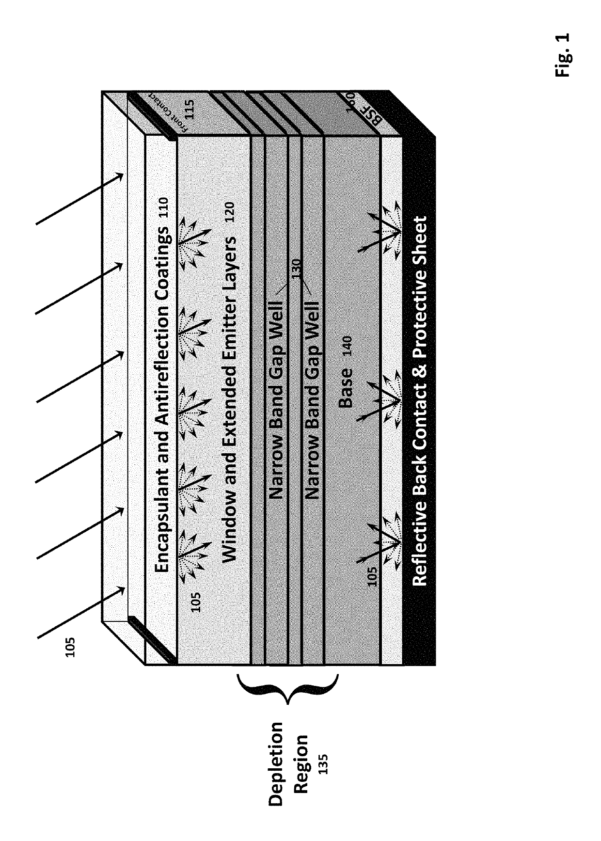
[0020]FIG. 1 details a cross-sectional view of an illustrative embodiment of a flexible, broadband photovoltaic sheet that incorporates various nano-inspired features. Incident photons 105 strike the top surface of an anti-reflective encapsulant structure 110 and are then transmitted into an underlying semiconductor window and extended emitter layer structure 120. The semiconductor base layer 140 is comprised of material with an energy gap that is less than or equal to the semiconductor material used in the window and extended emitter layers. The unabsorbed incident light 105 and photons emitted from the base layer structure 140 then pass through the higher energy gap back surface ...


PUM


Abstract

The invention described herein details flexible, high-efficiency photovoltaic cells with nano-enhanced absorbers and ultra-low dark current. By extending infrared absorption, power conversion efficiencies in single-junction, nano-enhanced solar cells can potentially meet or even exceed the Shockley-Queisser limit. Novel device designs utilizing advanced band gap engineering are employed to suppress non-radiative recombination and expose the limiting radiative component of the dark current. Light trapping structures and new nanostructured absorber designs are also considered to maximize the creation and collection of photogenerated carriers. Flexible photovoltaic devices are fabricated using established full-wafer epitaxial liftoff processes. The innovative design described herein provides for light-weight and flexible photovoltaic sheets capable of achieving ultra-high conversion efficiencies over a wide range of operating conditions.

Description

RELATED APPLICATIONS[0001]This application claims the benefit of U.S. Provisional Application Ser. No. 61 / 789,797, filed Mar. 15, 2013, entitled BROADBAND PHOTOVOLTAIC SHEETS AND METHOD OF CONSTRUCTING THE SAME, the entire disclosure of which is herein incorporated by reference. This application is also a continuation-in-part of, and claims the benefit of, co-pending U.S. patent application Ser. No. 12 / 985,921, filed Jan. 6, 2011, entitled CONCENTRATOR PHOTOVOLTAIC SUBASSEMBLY AND METHOD OF CONSTRUCTING THE SAME, the entire disclosure of which is herein incorporated by reference, which claims the benefit of U.S. Provisional Patent Application Ser. No. 61 / 293,469, filed on Jan. 8, 2010, entitled EFFICIENT SOLAR CELL EMPLOYING MULTIPLE ENERGY-GAP LAYERS AND LIGHT-SCATTERING STRUCTURES AND METHODS FOR CONSTRUCTING THE SAME, which is also expressly incorporated herein by reference.FIELD OF THE INVENTION[0002]This invention relates to semiconductor-based photovoltaic energy converters, a...

Claims


Application Information

Patent Timeline
Patent Type & Authority Patents(United States)
IPC IPC(8): H01L31/00H01L31/0352H01L31/18H01L29/12H01L33/44H01L33/46H01L31/0232H01L31/0304H01L31/0216
CPCH01L31/18H01L31/035236H01L31/02168H01L29/122H01L31/03046H01L31/02327H01L33/46H01L33/44H01L31/048H01L31/0735Y02E10/544
Inventor WELSER, ROGER E.SOOD, ASHOK K.
Owner MAGNOLIA OPTICAL TECH
Why Eureka
Try Eureka