

Adhesive composition, semiconductor device containing cured product thereof, and method for manufacturing semiconductor device using same
a technology of adhesive composition and semiconductor device, which is applied in the direction of polyether adhesive, semiconductor/solid-state device details, polyether adhesive, etc., can solve the problems of voids remaining in semiconductor devices, unrecognizable alignment marks, and inadequate solder wettability of joining sections after mounting, etc., to achieve excellent suppression of void generation and sufficient solder wettability of joining sections
- Summary
- Abstract
- Description
- Claims
- Application Information
AI Technical Summary
Benefits of technology
Problems solved by technology
Method used
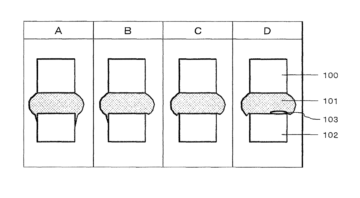
Image

Examples
examples
[0047]The present invention will be described in detail below with reference to examples, but these examples are not intended to limit the present invention.
[0048]
[0049]Each of the high-molecular compound and the epoxy compound was dissolved in N-methyl-2-pyrrolidone (hereinafter, referred to as NMP) to prepare a solution with a concentration of 0.1 wt %. The solution was used as a measurement sample. A weight average molecular weight on the polystyrene equivalent basis was calculated using a GPC apparatus Waters 2690 (manufactured by Waters Corporation), the configuration of which is as shown below. GPC measurement is performed by using NMP containing 0.05 mol / L of LiCl and 0.05 mol / L of phosphoric acid dissolved therein as a mobile layer at a flow rate of 0.4 mL / min. The column was heated to 40° C. using a column oven.
Detector: Waters 996
System controller: Waters 2690
Columns: TOSOH TSK-GEL α-4000
Columns: TOSOH TSK-GEL α-2500
[0050]
[0051]The particle diameters of 100 particles were ...
PUM
| Property | Measurement | Unit |
|---|---|---|
| particle diameter | aaaaa | aaaaa |
| particle diameter | aaaaa | aaaaa |
| viscosity | aaaaa | aaaaa |
Abstract
Description
Claims
Application Information