Copper alloy sheet material, connector, and method of producing a copper alloy sheet material

a technology of copper alloy sheet material and copper alloy sheet, which is applied in the direction of conductive materials, metal/alloy conductors, and conductors, etc., can solve the problems of permanent deformation of the material, increased contact resistance, and inability to obtain the desired contact pressure as a spring, etc., to achieve satisfactory bending workability, satisfactory electrical conductivity, and high yield strength

Active Publication Date: 2019-05-21
FURUKAWA ELECTRIC CO LTD
View PDF16 Cites 0 Cited by
  • Summary
  • Abstract
  • Description
  • Claims
  • Application Information

AI Technical Summary

Benefits of technology

[0023]The copper alloy sheet material of the present invention has characteristics in which a balance is achieved among high yield strength, satisfactory bending workability, and satisfactory electrical conductivity.
[0024]Therefore, the copper alloy sheet material of the present invention can be preferably used for: relays, switches, sockets and the like for electrical / electronic equipment; connectors, terminal materials and the like for automotive vehicles and the like; electroconductive spring materials to be used in electronic equipment components, such as auto-focus camera modules; connectors for flexible printed circuit (FPC); and the like.
[0025]Further, since the copper alloy sheet material of the present invention has high yield strength while having bending workability that is equivalent to that of conventional copper alloy sheet materials, the copper alloy sheet material of the invention can be used as a material for a spring, which is not apt to be permanent set in fatigue (resistance to settling). For this reason, the copper alloy sheet material is preferable, for example, as a connector material.
[0026]Further, according to the method of producing a copper alloy sheet material of the present invention, the copper alloy sheet material having the excellent characteristics described above can be produced preferably.

Problems solved by technology

When that stress becomes higher than the yield point of the copper alloy material, the material is permanently deformed, and the desired contact pressure as a spring may not be obtained.
In that case, the contact resistance is increased, and the electrical connection becomes insufficient, which becomes a serious problem.
Further, when each of individual terminals becomes small-sized, there is a problem that the cross-sectional area through which electricity flows is decreased, and a desired current cannot be passed through.
However, when the copper alloy has an alloying composition for high strength, the electrical conductivity is around 10% IACS, and this is insufficient for small-sized terminals.
Further, when an electronic instrument becomes small-sized, the thermal capacity is reduced, and when the amount of Joule heating of a conductor is high, this is directly related to the overall temperature elevation of the instrument, which is a problem.
However, the high strength (for example, high yield strength) and the satisfactory electrical conductivity described above are contradictory characteristics in a copper alloy.

Method used


Image

  • Copper alloy sheet material, connector, and method of producing a copper alloy sheet material
  • Copper alloy sheet material, connector, and method of producing a copper alloy sheet material

Examples


example 1

[0080]Raw materials of each alloy containing the alloying elements described in Table 1, with the balance being Cu and unavoidable impurities, were melted with a high-frequency melting furnace, and this was cast to obtain an ingot. The ingot was subjected to rollings at the rolling ratios described in the following steps, and thereby the size of the ingot was set to obtain the final sheet thickness (0.10 mm) without contradiction. Then, specimens of copper alloy sheet materials of Examples according to this invention and of Comparative Examples apart from those Examples, were respectively produced, by any one of the following production methods A, B, D, and E. Table 1 shows which production method among the methods A, B, D, and E was used. The final thickness of the copper alloy sheet material was set to 0.10 mm (100 μm). This final sheet thickness is also the same in the cases of production methods J, K, L, and M that will be described below, unless otherwise specified. The numbers...

example 2

[0104]Copper alloy sheet materials were produced using the copper alloys described in Table 2, and characteristics thereof were evaluated, by the same production methods and the same test and measurement methods as those used in Example 1. The results are presented in Table 2.

[0105]

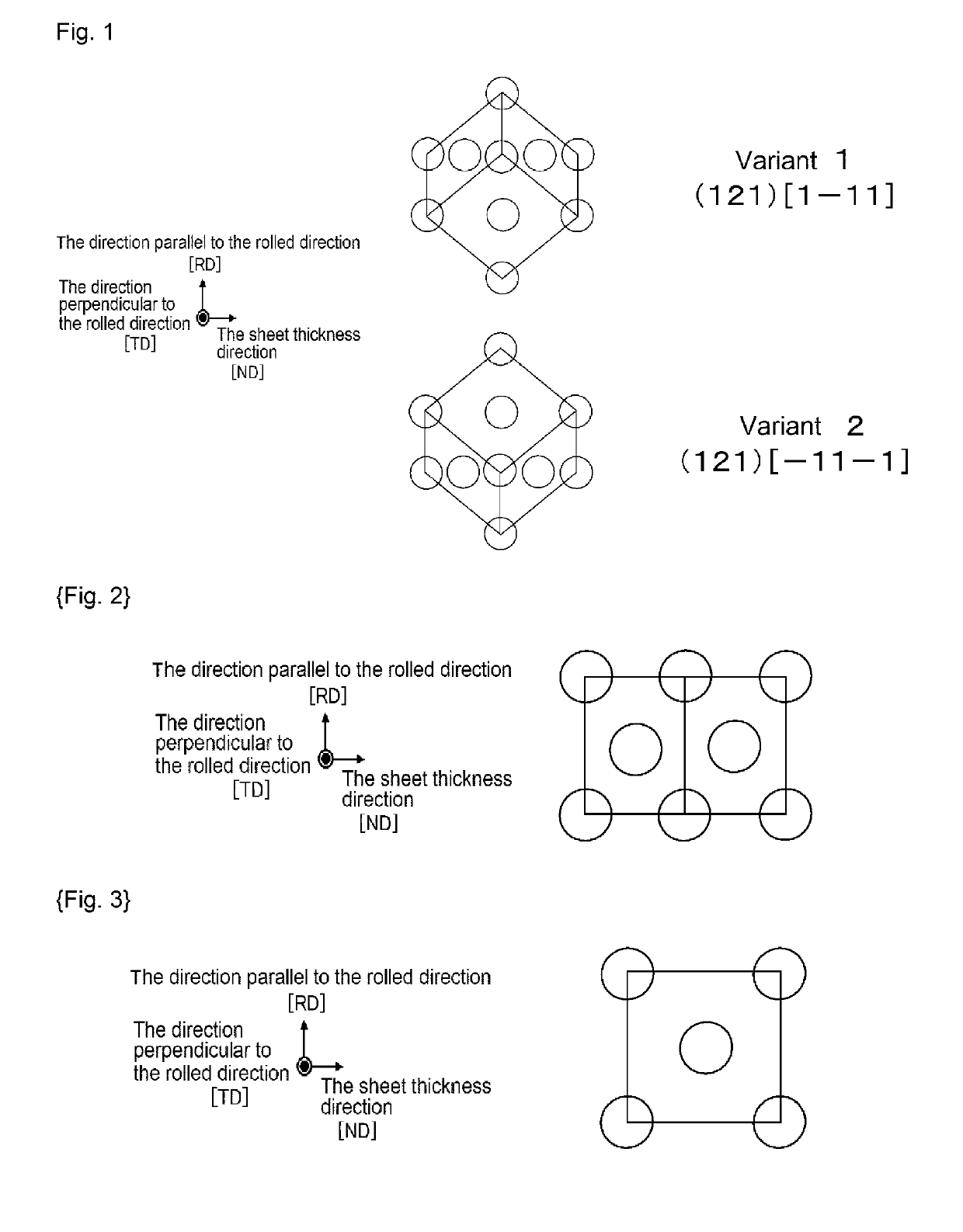
TABLE 2NiCoSiOther{121} {110} {001} mass mass mass elementsProduction orientationorientationorientation %%%mass %MethoddensitydensitydensityExample2011.84—0.45Zr = 0.11,A5 5 1Mn = 0.062022.64—0.59Mg = 0.15A3 7 02032.421.220.89Zn = 1.92A3 8 1Ag = 0.122043.78—0.91Mg = 0.08A210 02053.251.331.02Cr = 0.15A4 9 12064.65—1.13Mg = 0.12A211 02076.41—1.55Sn = 0.22B4 9 02087.88—1.83Fe = 0.23,B510 0P = 0.05Comparative2512.64—0.59Sn = 2.12Cracks of the material were occurred in rollingExample2523.81—0.91Mg = 0.15D4 3 12533.81—0.91Mg = 0.15E3 3 12543.81—0.91Mg = 0.15J4 2322553.81—0.91Mg = 0.15K3 5 12563.81—0.91Mg = 0.15L3 5 12573.81—0.91Mg = 0.15M3 1 2Density ρ of grainsYieldElectricalhaving {110} strengthBendingconduct...


PUM

PropertyMeasurementUnit
Young's modulusaaaaaaaaaa
temperatureaaaaaaaaaa
sizeaaaaaaaaaa

Abstract

A copper alloy sheet material, having an alloy composition containing at least one of Ni and Co in an amount of 1.80 to 8.00 mass % in total, Si in an amount of 0.40 to 2.00 mass %, and at least one element selected from the group consisting of Sn, Zn, Ag, Mn, P, Mg, Cr, Zr, Fe, and Ti in an amount of 0.000 to 2.000 mass % in total, with the balance being copper and unavoidable impurities, wherein the orientation density of the {121}<111> orientation is 6 or less, and the orientation density of the {110}<001> orientation is 4 or more; and wherein the density of grains having the {110}<001> orientation is 0.40 grains / μm2 or more; a connector using thereof; and a method of producing the copper alloy sheet material.

Description

CROSS-REFERENCE TO RELATED APPLICATIONS[0001]This application is a Continuation of PCT International Application No. PCT / JP2014 / 084432 filed on Dec. 25, 2014, which claims priority under 35 U.S.C. § 119 (a) to Japanese Patent Application No. 2013-273521 filed in Japan on Dec. 27, 2013. Each of the above applications is hereby expressly incorporated by reference, in its entirety, into the present application.TECHNICAL FIELD[0002]The present invention relates to a copper alloy sheet material and a connector using thereof, and a method of producing the copper alloy sheet material.BACKGROUND ART[0003]Along with making size of electric or electronic equipment smaller in recent years, making size of terminals and contact components smaller is underway. For example, in regard to an electrical contact, when the size of a member that constitutes a spring becomes small, the length of the spring is shortened, and thereby, the load stress applied to the copper alloy for spring is increased. Whe...

Claims


Application Information

Patent Timeline
Patent Type & Authority Patents(United States)
IPC IPC(8): C22F1/08B22D21/00H01B1/02C22C9/06C22C1/02
CPCC22F1/08B22D21/005H01B1/026C22C9/06C22C1/02C22C9/02C22C9/04C22C9/05C22C9/10
Inventor KANEKO, HIROSHI
Owner FURUKAWA ELECTRIC CO LTD
Why Eureka
Try Eureka