Semiconductor device

a technology of semiconductor devices and semiconductors, applied in the field of semiconductor devices, can solve the problems of more complicated and smaller circuit designs in the products of the new generation, and achieve the effects of improving the reliability of the semiconductor device, improving the electrical field unbalance of the transistor, and improving the operation performance and reliability

Active Publication Date: 2019-07-16
UNITED MICROELECTRONICS CORP
View PDF3 Cites 3 Cited by
  • Summary
  • Abstract
  • Description
  • Claims
  • Application Information

AI Technical Summary

Benefits of technology

[0003]A semiconductor device is provided in the present invention. A diode structure is applied to connect a gate electrode of a transistor and a substrate, and another diode structure is applied to connect a drain electrode of the transistor and the substrate for improving electrical field unbalance in the transistor. The operation performance and the reliability of the semiconductor device may be improved accordingly.

Problems solved by technology

The development of semiconductor integrated circuit technology progresses continuously and circuit designs in products of the new generation become smaller and more complicated than those of the former generation.
However, many other active or passive devices are also designed to be formed by the BEOL process as the required integrity of the integrated circuits becomes higher and higher, and many operation problems of the devices are generated and have to be solved accordingly.

Method used


Image

  • Semiconductor device
  • Semiconductor device
  • Semiconductor device

Examples


Embodiment Construction

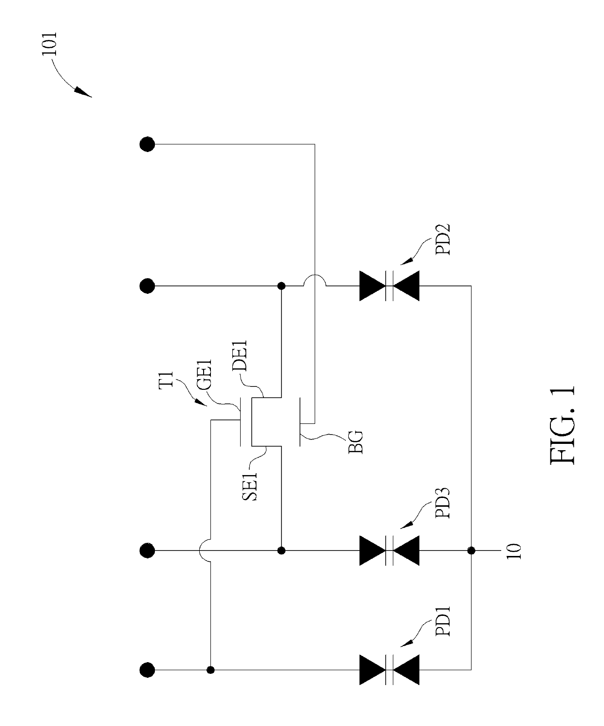
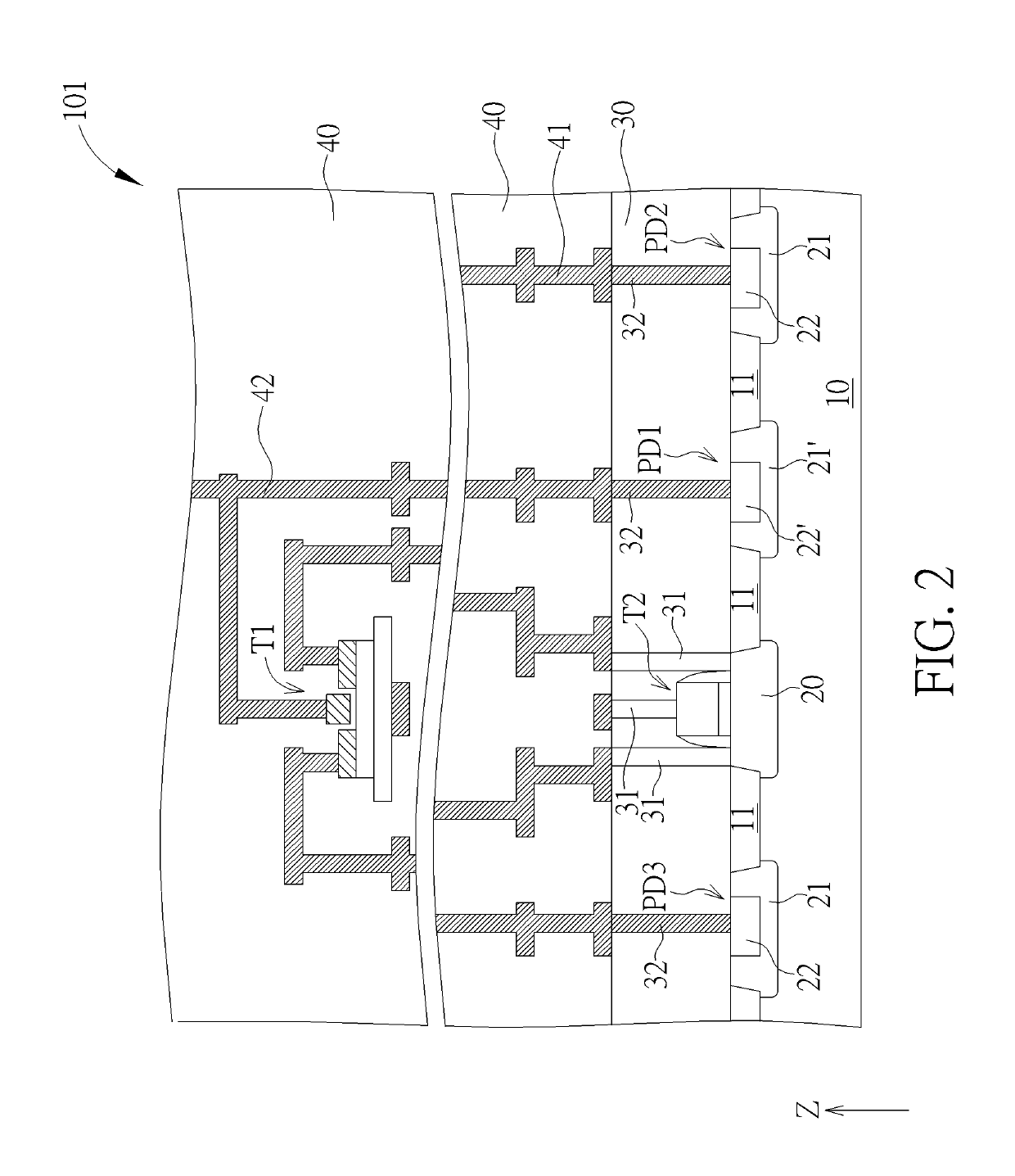
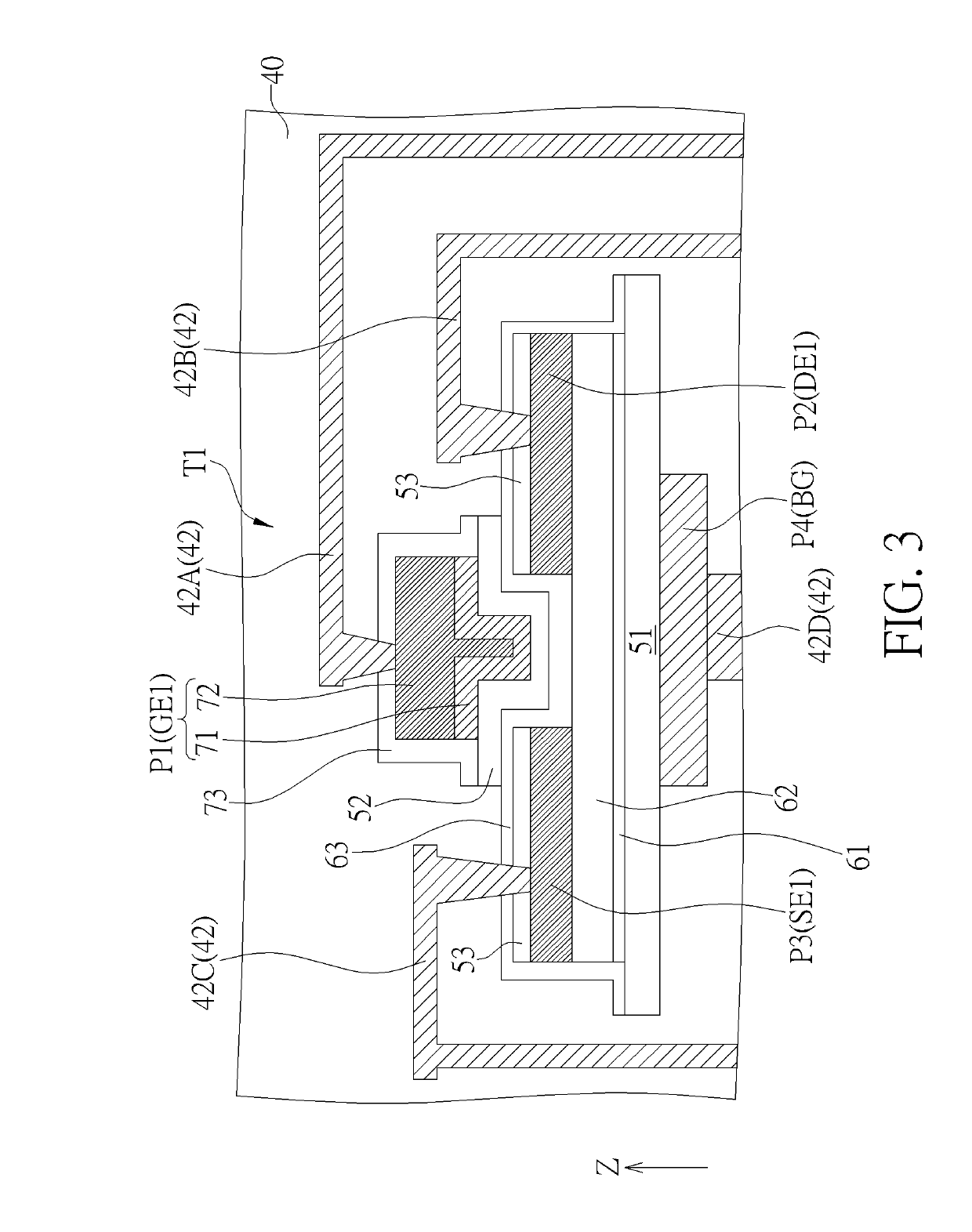
[0012]Please refer to FIG. 1, FIG. 2, and FIG. 3. FIG. 1 is a schematic circuit diagram of a semiconductor device according to a first embodiment of the present invention. FIG. 2 is a schematic drawing illustrating the semiconductor device in this embodiment. FIG. 3 is a partial enlarged view of the semiconductor device in this embodiment. As shown in FIG. 1, FIG. 2, and FIG. 3, a semiconductor device 101 is provided in this embodiment. The semiconductor device 101 includes a substrate 10, a first transistor T1, a first diode structure PD1, and a second diode structure PD2. The first transistor T1 is disposed on the substrate 10. The first transistor T1 includes a first gate electrode GE1, a first source electrode SE1, and a first drain electrode DE1. The first gate electrode GE1 is connected to the substrate 10 by the first diode structure PD1, and the first drain electrode DE1 is connected to the substrate 10 by the second diode structure PD2. In some embodiments, the semiconducto...


PUM


Abstract

A semiconductor device includes a substrate, a first transistor, a first diode structure, and a second diode structure. The first transistor is disposed on the substrate. The first transistor includes a first gate electrode, a first source electrode, and a first drain electrode. The first gate electrode is connected to the substrate by the first diode structure. The first drain electrode is connected to the substrate by the second diode structure. The first diode structure and the second diode structure may be used to improve potential unbalance in the transistor, and operation performance and reliability of the semiconductor device may be enhanced accordingly.

Description

BACKGROUND OF THE INVENTION1. Field of the Invention[0001]The present invention relates to a semiconductor device, and more particularly, to a semiconductor device including a diode structure.2. Description of the Prior Art[0002]The development of semiconductor integrated circuit technology progresses continuously and circuit designs in products of the new generation become smaller and more complicated than those of the former generation. The amount and the density of the functional devices in each chip region are increased constantly according to the requirements of innovated products, and the size of each device has to become smaller accordingly. The general semiconductor manufacturing process may be roughly divided into a front end of line (FEOL) process for forming transistors on a wafer and a back end of line (BEOL) process for forming parts such as contact structures, interlayer dielectric layers, interconnection structures, and contact pads above the transistors. However, man...

Claims


Application Information

Patent Timeline
Patent Type & Authority Patents(United States)
IPC IPC(8): H01L27/12H01L29/861H01L29/786H01L27/092H01L27/06H01L23/528
CPCH01L27/1207H01L27/0629H01L27/092H01L29/78666H01L23/5286H01L29/7869H01L29/78648H01L29/8611H01L29/78675H01L27/0688H01L21/8258H01L27/1225H01L29/861
Inventor LI, XIANGCHEN, DING-LUNGTUNG, YU-CHENG
Owner UNITED MICROELECTRONICS CORP
Why Eureka
Try Eureka