
MicroLED display panel

a display panel and micro-chip technology, applied in the field of display panels, can solve the problems of thermal mismatch, significantly affected, and more complex than flip chip technology, and achieve the effects of reducing the loading of drivers, simplifying the process of making display panels, and reducing the turn-on time of micro-chips

Active Publication Date: 2019-07-16
PRILIT OPTRONICS INC
View PDF18 Cites 2 Cited by
  • Summary
  • Abstract
  • Description
  • Claims
  • Application Information

AI Technical Summary

Benefits of technology

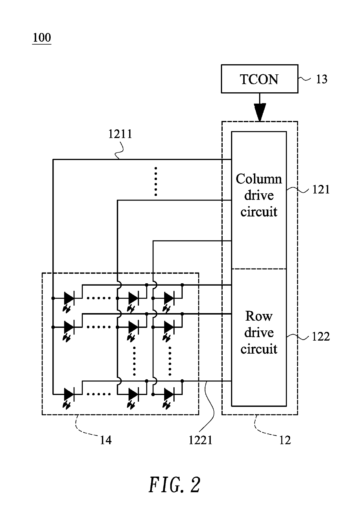
[0007]In view of the foregoing, it is an object of the embodiment of the present invention to provide a microLED display panel capable of effectively reducing loading of drivers, thereby making whole large-size high-resolution microLED display panel feasible. Passive driving scheme is adopted in one embodiment to simplify the process of making display panels, reduce turn-on time of the microLEDs, increase drive current, and effectively minimize effect on gray display due to leakage current.

Problems solved by technology

However, microLED is made by flip chip technology, while TFT is made by complementary metal-oxide-semiconductor (CMOS) process which is more complex than flip chip technology.
These two distinct technologies may cause thermal mismatch.
A drive current of the microLED is small in gray display, which may be significantly affected by leakage current.
When the size or the resolution of the display panel increases, output loading and delay of the drive circuits increase accordingly, causing the display panel to malfunction.
Therefore, passive matrix is not suitable for large-size microLED display panels.

Method used


Image

  • MicroLED display panel
  • MicroLED display panel
  • MicroLED display panel

Examples


Embodiment Construction

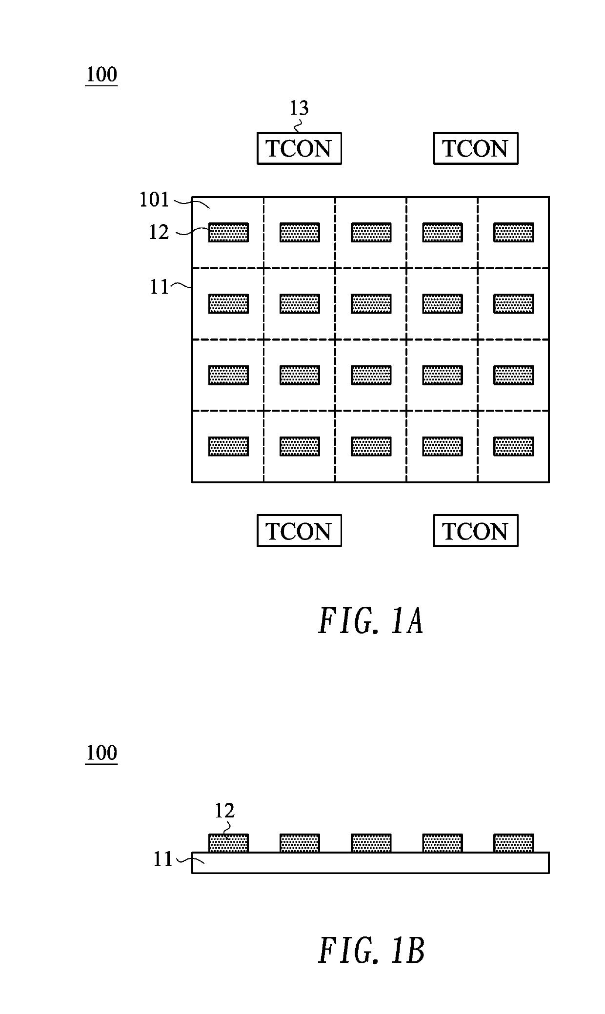
[0016]FIG. 1A shows a top view illustrated of a micro light-emitting diode (microLED) display panel 100 according to one embodiment of the present invention, and FIG. 1B shows a side view illustrated of the microLED display panel 100 of FIG. 1A. The microLED display panel of the embodiment is preferably adaptable to a large-size and high-resolution (e.g., 3840RGB×2160) display panel. In the specification, the size range of the microLED is between 1 and 10 micrometers. However, the size of the microLED may be even smaller due to specific applications or technological advance. In the specification, “large-size” display panel is currently and commonly referred to 10 inches or above display panel. However, “large-size” display panel may be referred to other display size due to specific applications or technological advance. In the specification, “high-resolution” display panel is currently and commonly referred to a display panel with 1080 or above scan lines. However, “high-resolution”...


PUM


Abstract

A microLED display panel includes a substrate being divided into a plurality of sub-regions for supporting microLEDs, and a plurality of drivers being correspondingly disposed on surfaces of the sub-regions respectively. The driver includes a low-dropout (LDO) regulator and a drive circuit. The LDO regulator receives a system power, according to which a regulated power is generated and provided for the drive circuit.

Description

CROSS-REFERENCE TO RELATED APPLICATIONS[0001]This application claims priority of Taiwan Application No. 105131054, filed on Sep. 26, 2016, and Taiwan Application No. 106118892, filed on Jun. 7, 2017, the entire contents of which are hereby incorporated by reference.BACKGROUND OF THE INVENTION1. Field of the Invention[0002]The present invention generally relates to a display panel, and more particularly to a microLED display panel.2. Description of Related Art[0003]A micro light-emitting diode (microLED, mLED or μ LED) display panel is one of flat display panels, which is composed of microscopic microLEDs each of a size of 1-10 micrometers. Compared to conventional liquid crystal display panels, the microLED display panels offer better contrast, response times and energy efficiency. Although both organic light-emitting diodes (OLEDs) and microLEDs possess good energy efficiency, the microLEDs, based on group III / V (e.g., GaN) LED technology, offer higher brightness, higher luminous e...

Claims


Application Information

Patent Timeline
Patent Type & Authority Patents(United States)
IPC IPC(8): G09F9/33H05B33/08G09F1/00H01L25/075H01L25/16H05K1/03H05B44/00
CPCH05B33/0815G09F1/00G09F9/33H01L25/0753H05K2201/10106H01L25/167H05K1/0306H05K2201/10053G09G3/32H05B45/37
Inventor WU, BIING-SENGCHEN, FA-MING
Owner PRILIT OPTRONICS INC
Learn More