UV light emitting device

a light emitting device and ultraviolet light technology, applied in the direction of semiconductor devices, basic electric elements, electrical appliances, etc., can solve the problems of significant deterioration in luminous efficacy of the light emitting device, lattice mismatch or difference in thermal expansion coefficient, and the cracking or breaking so as to improve the crystallinity of the semiconductor layer and improve the reliability and efficiency of the uv light emitting device.

Active Publication Date: 2019-08-06
SEOUL VIOSYS CO LTD
View PDF31 Cites 0 Cited by
  • Summary
  • Abstract
  • Description
  • Claims
  • Application Information

AI Technical Summary

Benefits of technology

[0009]According to exemplary embodiments, a UV light emitting device includes an anti-cracking layer disposed on a first conductive type semiconductor layer to improve crystallinity of semiconductor layers, thereby improving reliability and efficiency of the UV light emitting device. In addition, according to exemplary embodiments, a method of fabricating a UV light emitting device includes forming an anti-cracking layer on a first conductive type semiconductor layer, thereby facilitating separation of a growth substrate from the first conductive type semiconductor layer.

Problems solved by technology

Then, the light emitting device suffers from significant deterioration in luminous efficacy.
However, when AlxGa(1-x)N layer (0.1≤×≤1) containing 10% or more of Al is grown on the sapphire substrate, the UV light emitting device suffers from cracking or breaking caused by thermal or structural deformation due to a high Al content.
This problem is caused by lattice mismatch or difference in coefficient of thermal expansion between the sapphire substrate and the AlxGa(1-x)N layer (0.1≤×≤1).
Due to bowing of the wafer, cracks are generated in the nitride semiconductor, thereby causing deterioration in production yield and quality of light emitting devices.

Method used


Image

  • UV light emitting device
  • UV light emitting device
  • UV light emitting device

Examples


Embodiment Construction

[0016]A UV light emitting device according to various exemplary embodiments and a method of fabricating the same can be realized in various ways.

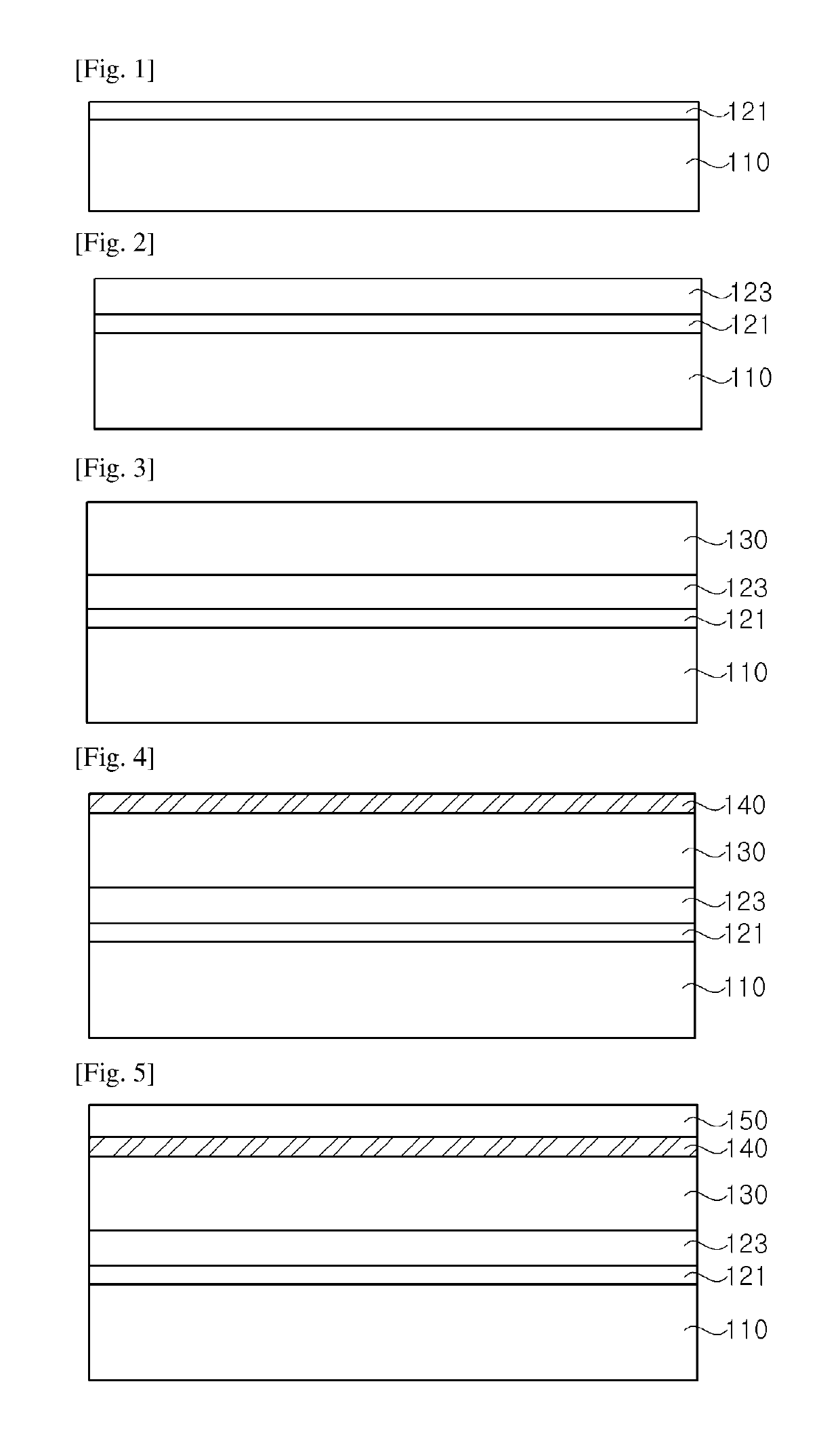
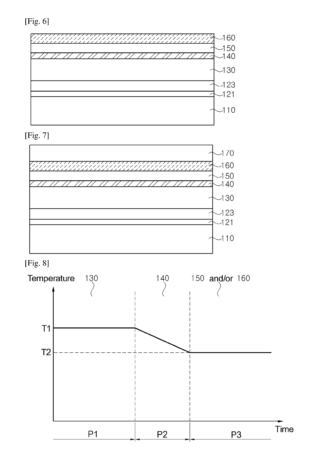
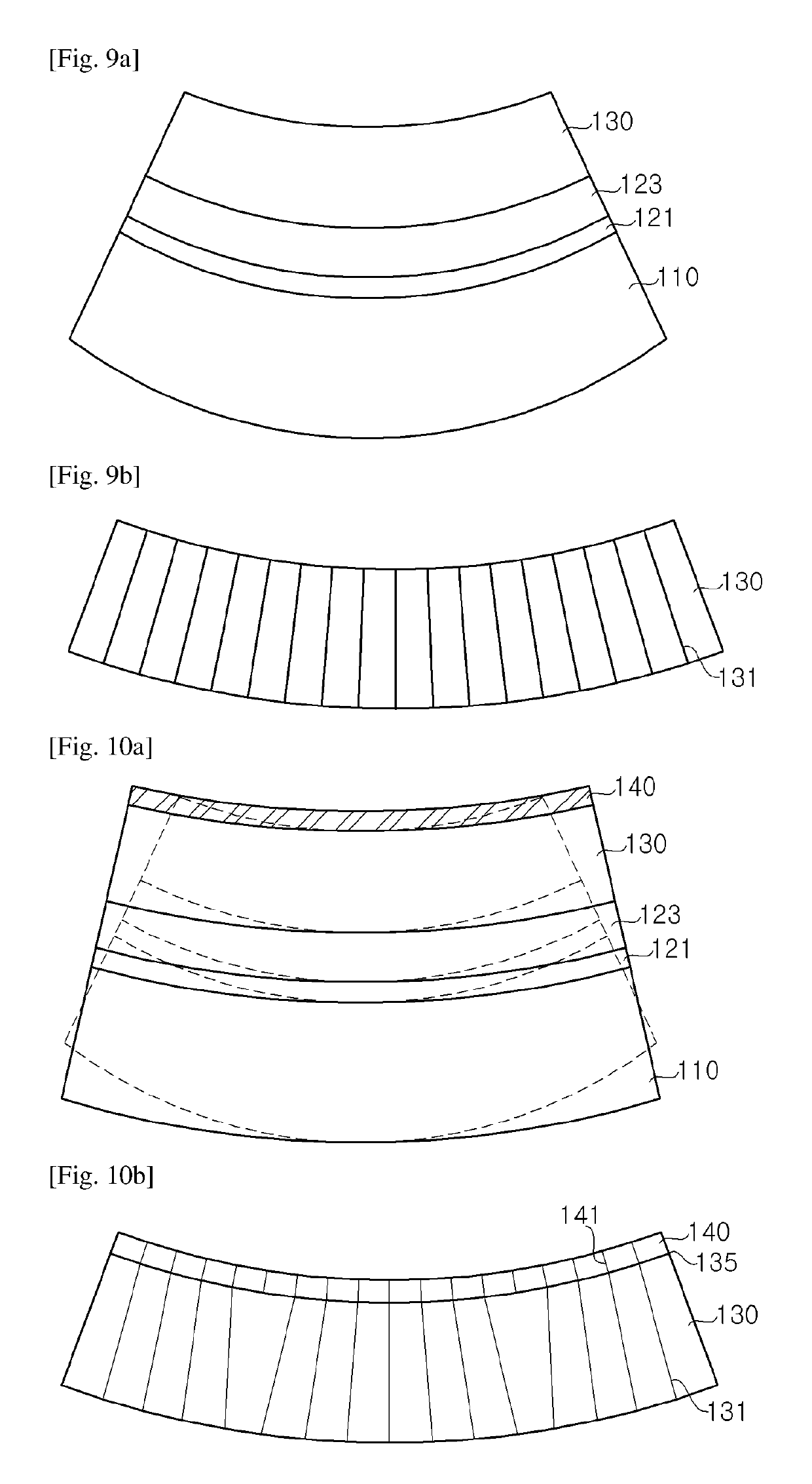
[0017]A UV light emitting device according to some exemplary embodiments includes a first conductive type semiconductor layer; an anti-cracking layer disposed on the first conductive type semiconductor layer; an active layer disposed on the anti-cracking layer; and a second conductive type semiconductor layer disposed on the active layer, wherein the anti-cracking layer includes first lattice points and second lattice points disposed at an interface between the first conductive type semiconductor layer and the anti-cracking layer, the first lattice points are connected to lattices of the first conductive type semiconductor layer, and the second lattice points are not connected to the lattices of the first conductive type semiconductor layer.

[0018]At the interface between the first conductive type semiconductor layer and the anti-cracking la...


PUM


Abstract

Disclosed herein is a UV light emitting device. The UV light emitting device includes a first conductive type semi-conductor layer, an anti-cracking layer disposed on the first conductive type semiconductor layer, an active layer disposed on the anti-cracking layer, and a second conductive type semiconductor layer disposed on the active layer, wherein the anti-cracking layer includes first lattice points and second lattice points disposed at an interface between the first conductive type semiconductor layer and the anti-cracking layer, the first lattice points are connected to lattices of the first conductive type semiconductor layer, and the second lattice points are not connected to the lattices of the first conductive type semiconductor layer.

Description

TECHNICAL FIELD[0001]Exemplary embodiments of the present disclosure relate to an ultraviolet (UV) light emitting device, and more particularly, to a UV light emitting device including an anti-cracking layer capable of preventing generation of cracks to improve crystallinity of semiconductor layers.BACKGROUND ART[0002]Since a UV light emitting device emits light having a relatively short peak wavelength (generally, a peak wavelength of 400 nm or less), a light emitting region is formed of AlGaN containing 10% or more of Al in fabrication of a UV light emitting device using a nitride semiconductor. In such a UV light emitting device, if n-type and p-type nitride semiconductor layers have smaller energy band-gaps than energy of UV light emitted from an active layer, UV light emitted from the active layer can be absorbed into the n-type and p-type nitride semiconductor layers in the light emitting device. Then, the light emitting device suffers from significant deterioration in luminou...

Claims


Application Information

Patent Timeline
Patent Type & Authority Patents(United States)
IPC IPC(8): H01L33/12H01L33/22H01L33/06H01L33/00H01L33/32
CPCH01L33/12H01L33/007H01L33/32H01L33/06H01L33/22H01L33/0079H01L33/0093
Inventor HAN, CHANG SEOKKWAK, WOO CHULCHOI, HYO SHIKHWANG, JUNG HWANJANG, CHANG GEUN
Owner SEOUL VIOSYS CO LTD
Why Eureka
Try Eureka