Model-based metrology using images

a model-based metrology and image technology, applied in the field of model-based measurements, can solve the problems of inability to reliably perform traditional image-based metrology algorithms with arbitrary targets or device structures, and the number of locations that can be measured for a given wafer throughput requirement is limited, so as to achieve the effect of quick and accurate estimation of structural parameters

Active Publication Date: 2019-08-13
KLA CORP
View PDF32 Cites 2 Cited by
  • Summary
  • Abstract
  • Description
  • Claims
  • Application Information

AI Technical Summary

Benefits of technology

[0009]Methods and systems for combining the information content present in measured images of semiconductor wafers with additional measurements of particular structures within the measured images to quickly and accurately estimate structural parameters of interest are presented herein.
[0010]In one aspect, the high information content present in measured images is transformed into estimated values of structural parameters of interest. An image-based signal response metrology (SRM) model is trained based on measured, image-based training data (e.g., images collected from a Design of Experiments (DOE) wafer) and corresponding reference measurement data. The trained, image-based measurement model is then used to calculate values of one or more parameters of interest directly from measured image data collected from other wafers. The trained, image-based SRM models described herein receive image data directly as input and provide estimates of values of one or more parameters of interest as output. By streamlining the measurement process, the predictive results are improved along with a reduction in computation and user time.
[0011]By using only raw image data to create the image-based measurement model, as described herein, the errors and approximations associated with traditional image based metrology methods are reduced. In addition, the image-based measurement model is not sensitive to systematic errors, asymmetries, etc. because the image-based measurement model is trained based on image data collected from a particular metrology system and used to perform measurements based on images collected from the same metrology system.
[0012]In another aspect, measured images are transformed into synthetic non-imaging based measurement signals associated with a model-based measurement technique at one or more locations a field. The model-based measurement technique is employed to estimate values of structural parameters of interest based on the synthetic signals. A measurement signal synthesis model is trained based on measured, image-based training data (e.g., images collected from a Design of Experiments (DOE) wafer) and corresponding non-imaging measurement data. In a further aspect, synthetic signals are generated for multiple structures in different locations in each imaged field. In some examples, performing model based measurements based on the synthetic signals is significantly faster than acquiring actual measurement data at each different location.

Problems solved by technology

Although non-imaging, model-based optical metrology techniques offer high precision measurement capability, the number of locations that can be measured for a given wafer throughput requirement is limited.
Unfortunately, at this time, imaging-based measurements lack sufficient resolution to directly measure complex three dimensional structures that are commonly manufactured today.
For this reason, traditional image based metrology algorithms cannot perform reliably with arbitrary targets or device structures.
The measurement of dedicated metrology structures by traditional scatterometry based metrology techniques is time consuming.
Future metrology applications present challenges for image based metrology due to increasingly small resolution requirements and the increasingly high value of wafer area.

Method used


Image

  • Model-based metrology using images
  • Model-based metrology using images
  • Model-based metrology using images

Examples


Embodiment Construction

[0024]Reference will now be made in detail to background examples and some embodiments of the invention, examples of which are illustrated in the accompanying drawings.

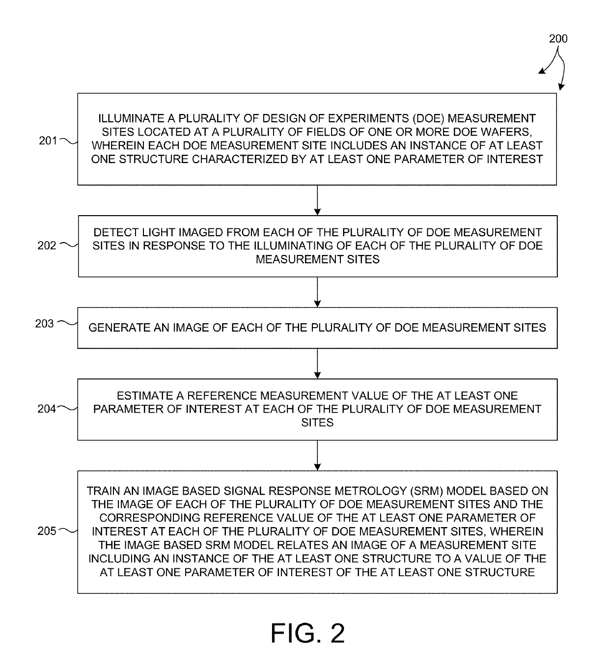
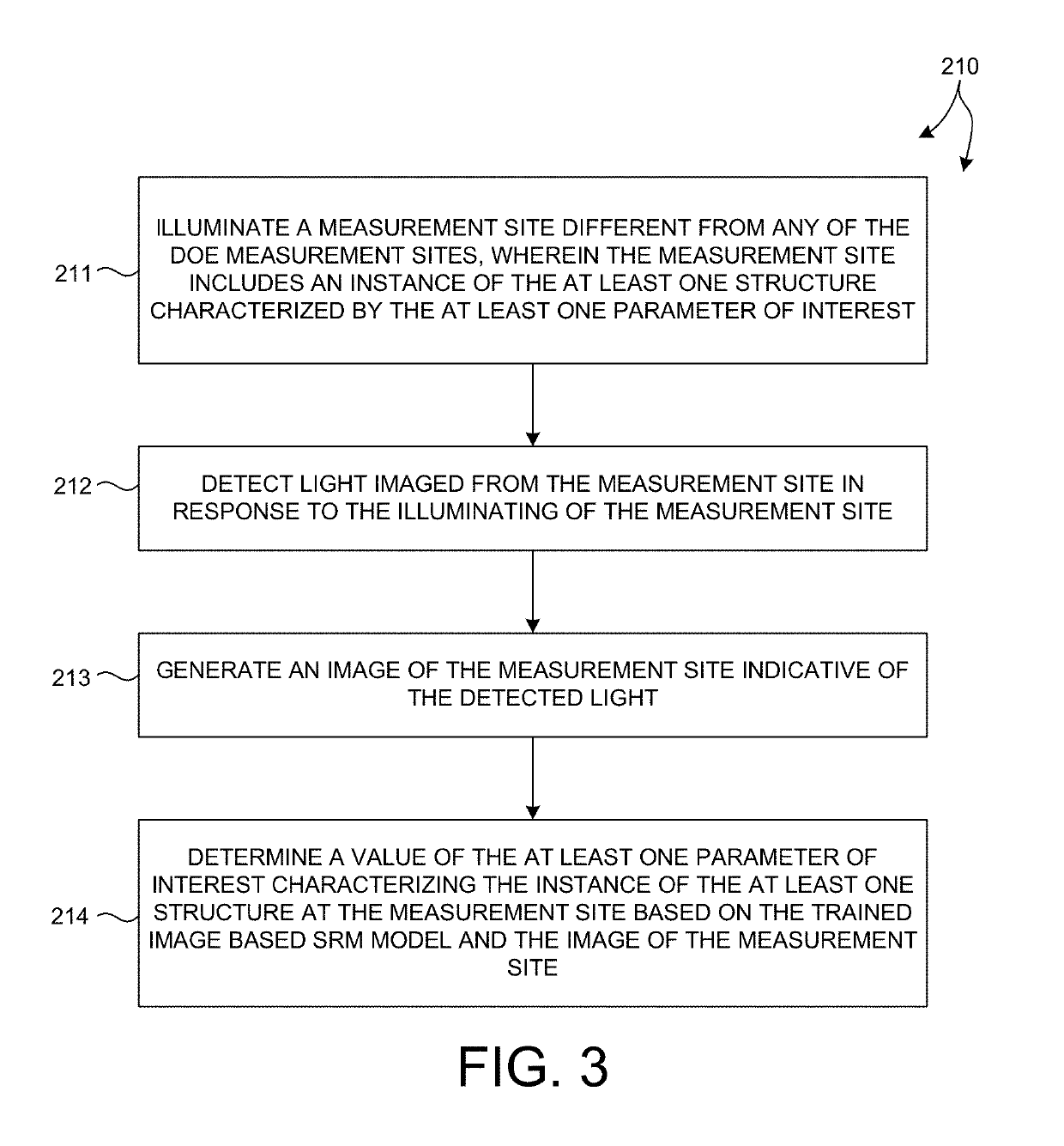
[0025]Methods and systems for combining the information content present in measured images of semiconductor wafers with additional measurements of particular structures within the measured images to quickly and accurately estimate structural parameters of interest are presented herein.

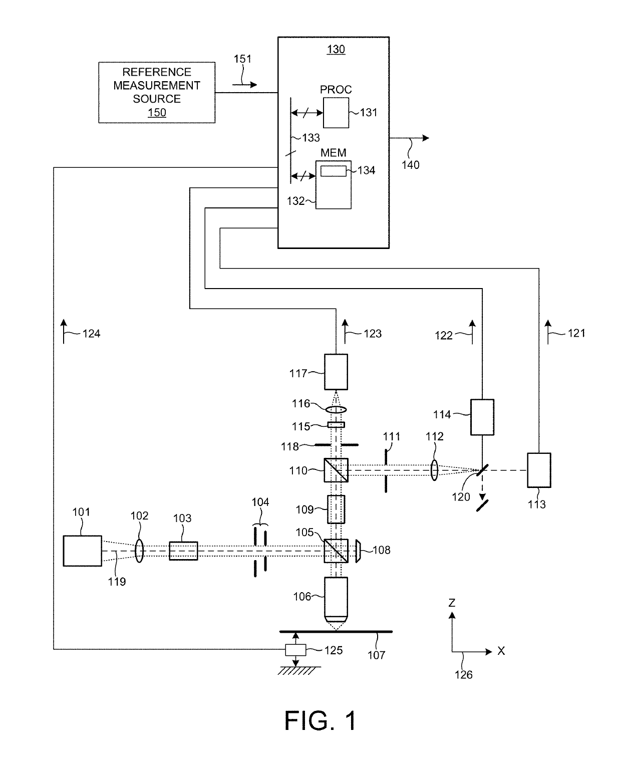
[0026]FIG. 1 illustrates a system 100 for measuring characteristics of a specimen in accordance with the exemplary methods presented herein. As shown in FIG. 1, the system 100 may be used to perform imaging and non-imaging measurements of one or more structures formed on a specimen 107. In this aspect, the system 100 may configured as a beam profile reflectometer (BPR), a field imaging system, and a spectroscopic reflectometer (SR). Alternatively, system 100 may be configured as a BPR, a spectroscopic ellipsometer (SE), and a field imagi...


PUM

PropertyMeasurementUnit
sizeaaaaaaaaaa
dimensionaaaaaaaaaa
critical dimensionaaaaaaaaaa

Abstract

Methods and systems for combining information present in measured images of semiconductor wafers with additional measurements of particular structures within the measured images are presented herein. In one aspect, an image-based signal response metrology (SRM) model is trained based on measured images and corresponding reference measurements of particular structures within each image. The trained, image-based SRM model is then used to calculate values of one or more parameters of interest directly from measured image data collected from other wafers. In another aspect, a measurement signal synthesis model is trained based on measured images and corresponding measurement signals generated by measurements of particular structures within each image by a non-imaging measurement technique. Images collected from other wafers are transformed into synthetic measurement signals associated with the non-imaging measurement technique and a model-based measurement is employed to estimate values of parameters of interest based on the synthetic signals.

Description

CROSS REFERENCE TO RELATED APPLICATION[0001]The present application for patent claims priority under 35 U.S.C. § 119 from U.S. provisional patent application Ser. No. 62 / 212,113, entitled “Model-Based Metrology Using Images,” filed Aug. 31, 2015, the subject matter of which is incorporated herein by reference in its entirety.TECHNICAL FIELD[0002]The described embodiments relate to metrology systems and methods, and more particularly to methods and systems for improved model-based measurements.BACKGROUND INFORMATION[0003]Semiconductor devices such as logic and memory devices are typically fabricated by a sequence of processing steps applied to a specimen. The various features and multiple structural levels of the semiconductor devices are formed by these processing steps. For example, lithography among others is one semiconductor fabrication process that involves generating a pattern on a semiconductor wafer. Additional examples of semiconductor fabrication processes include, but are...

Claims


Application Information

Patent Timeline
Patent Type & Authority Patents(United States)
IPC IPC(8): G03F7/20G06K9/52G06K9/62G06T7/00H04N17/00H04N5/225
CPCG06T7/0004G03F7/70625G03F7/70633G06K9/522G06K9/624H04N17/002G06K9/6269G06K9/6282G06T2207/20081G06T2207/30148H04N5/2256G06K9/6247G01N21/9501G01N21/9515G06T7/001G06V10/431G06V20/66H04N23/56G06F18/2134G06F18/2135G06F18/2411G06F18/24323
Inventor PANDEV, STILIAN IVANOV
Owner KLA CORP
Why Eureka
Try Eureka