Display device and method of driving same

a display device and display technology, applied in the direction of measurement devices, static indicating devices, instruments, etc., can solve the problems of image sticking, degrading display quality, and difficult to increase the screen size and achieve high definition, so as to reduce the influence of noise, reduce the influence of compensation computation, and improve the conventional sn ratio of data used

Active Publication Date: 2019-08-20
SHARP KK
View PDF8 Cites 0 Cited by
  • Summary
  • Abstract
  • Description
  • Claims
  • Application Information

AI Technical Summary

Benefits of technology

[0038]According to the first or ninth phase of the present invention, the display device includes a current measuring unit configured to measure a current flowing through a circuit element and an average value calculation unit configured to calculate an average value of a plurality of input values. In this configuration, the current measuring unit performs current monitoring on each pixel a plurality of times (rounds) in a fixed amount of time, and the average value calculation unit calculates an average value of measured values obtained in the plurality of rounds of current monitoring. Compensation computation can thus be performed, for example, to compensate for variations in threshold voltage of drive transistors and degradation of organic EL elements by using data on the average value of measured values obtained in the plurality of rounds of current monitoring. By virtue of LPF (low-pass filtering) effect for each pixel over time, such use of average value data improves on the conventional SN ratio of the data used in compensation computation even when the current data obtained by the current monitoring is prone to noise. In other words, when noise occurs during current monitoring, the noise has less influence on the compensation computation. Hence, the present invention, in the first or ninth phase thereof, provides a display device that is capable of suppressing influence of noise in detecting a current for compensation for degradation of a circuit element (e.g., a drive transistor or an organic EL element).
[0039]According to the second phase of the present invention, the control circuit transmits data on the average value to the external device. Therefore, the total amount of data transferred from the control circuit to the external device can be reduced.
[0040]According to the third phase of the present invention, the display device transmits data on the average value to the external device at a reduced data transfer rate. Therefore, desirable compensation computation can be performed based on results of current monitoring even when the data transfer bandwidth from the display device to the external device is narrow.
[0041]According to the fourth phase of the present invention, there is provided a line memory having a plurality of ports in the control circuit, which enables the data transfer rate from the display device to the external device to be readily reduced.
[0042]According to the fifth phase of the present invention, the amount of data transferred from the data line drive circuit to the control circuit can be reduced.
[0043]According to the sixth phase of the present invention, because the control circuit for the display device is generally a large scale integrated circuit, the average value calculation unit can be readily provided in the control circuit.

Problems solved by technology

The organic EL display device driven by a passive matrix method has a simple structure, but difficult to increase the screen size and achieve high definition.
The numerous drive transistors in the display unit, having various threshold voltages, result in variable luminance, thereby degrading display quality.
This phenomenon causes image sticking.

Method used


Image

  • Display device and method of driving same
  • Display device and method of driving same
  • Display device and method of driving same

Examples


first embodiment

1. First Embodiment

1.1 Overall Configuration

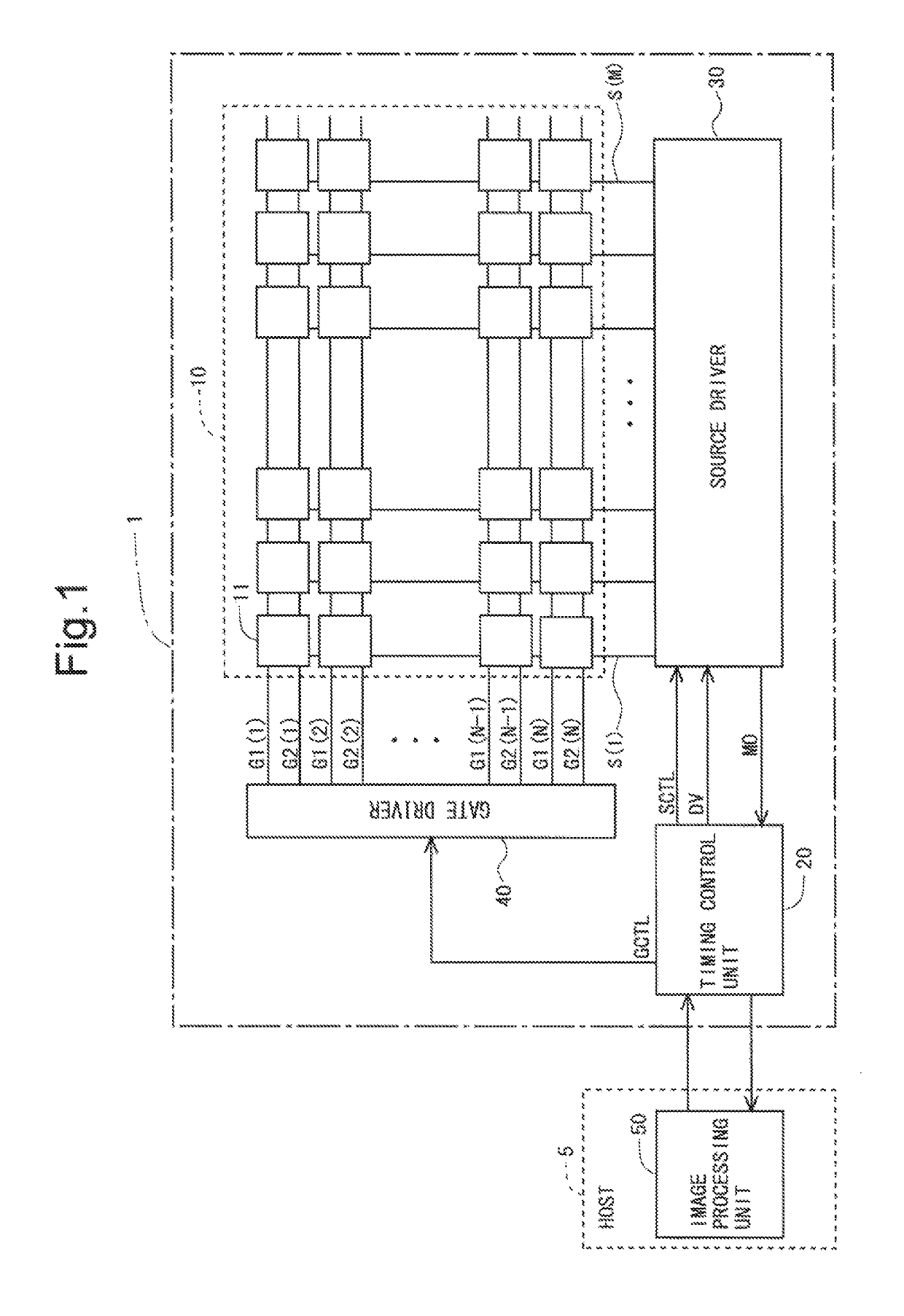
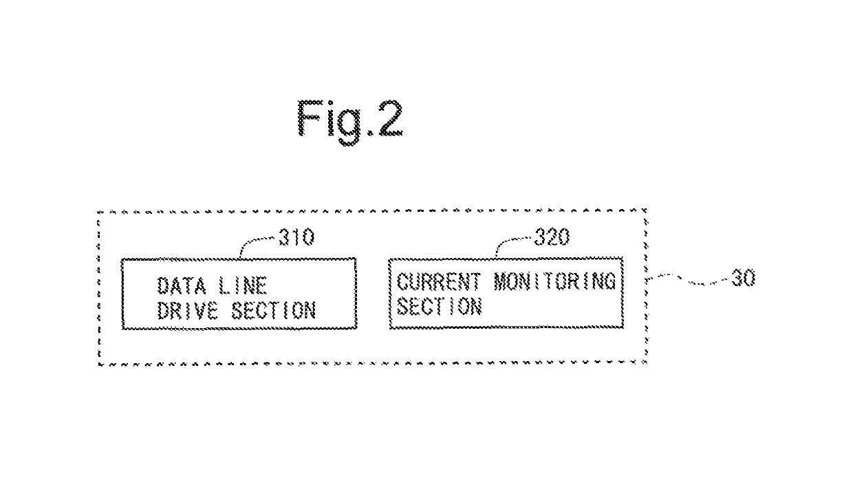
[0072]FIG. 1 is a block diagram of an overall configuration of an active-matrix organic EL display device 1 in accordance with a first embodiment of the present invention. The organic EL display device 1 includes a display unit 10, a timing control unit 20, a source driver 30, and a gate driver 40. The source driver 30, as shown in FIG. 2, includes a portion that functions as a data line drive section 310 and a portion that functions as a current monitoring section 320. Either one of the source driver 30 and the gate driver 40 or both may be formed integrally with the display unit 10. The organic EL display device 1 exchanges data with an image processing unit 50 in a host (e.g., a main body of a personal computer) 5.

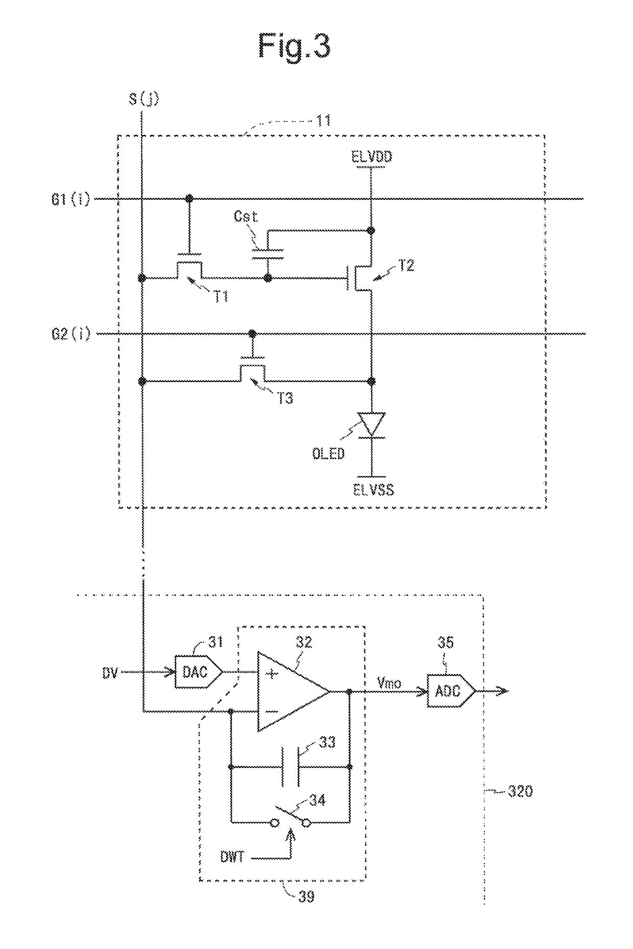
[0073]The display unit 10 includes M data lines S(1) to S(M) and N scan lines G1(1) to G1(N) disposed at right angles. The display unit 10 further includes N monitoring control lines G2(1) to G2(N) each associated with a diffe...

second embodiment

2. Second Embodiment

2.1 Configuration

[0110]Now, a second embodiment of the present invention will be described. The description will focus on differences from the first embodiment above; no description will be repeated on those respects which are similar to the first embodiment. The averaging section in the first embodiment is disposed in the current monitoring section 320 in the source driver 30. In contrast, in the present embodiment, the averaging section is disposed in the timing control unit 20.

[0111]FIG. 16 is a block diagram of a functional configuration of the current monitoring section 320 in accordance with the present embodiment. As shown in FIG. 16, the current monitoring section 320 includes a current / voltage conversion section 39 and an AD converter 35. The current / voltage conversion section 39 converts a monitored current Imo to a voltage (monitored voltage) Vmo. The AD converter 35 converts this analog monitored voltage Vmo to digital measured value data. Unlike the ...

third embodiment

3. Third Embodiment

3.1 Configuration

[0117]A third embodiment of the present invention will be described. The description will focus on differences from the first embodiment above; no description will be repeated on those respects which are similar to the first embodiment. Current monitoring is performed row by row in the first embodiment. This is why the line memory 37 is used in averaging. In contrast, in the present embodiment, current monitoring is performed sequentially from one pixel (pixel circuit) to another. In other words, current monitoring is repeated a plurality of times sequentially from one pixel to another. Flip-flops that serve as a memory unit for each pixel are used for this purpose in averaging. Current monitoring may be performed on each pixel any number of times (rounds) and in the present embodiment, repeated four times (rounds).

[0118]FIG. 19 is a diagram of a configuration of an averaging section 76 in accordance with the present embodiment. As shown in FIG. 1...


PUM


Abstract

The organic EL display device includes: a current monitoring section that measures a current flowing in a circuit element and outputs a digital measured value in accordance with the measured current; and an averaging section (36) that calculates an average value of a plurality of input values. The current monitoring section measures the current flowing in a circuit element in each pixel circuit a plurality of times in a fixed amount of time. For each pixel circuit, the averaging section (36) receives a plurality of measured values outputted from the current monitoring section in a fixed amount of time as a plurality of input values and outputs an average value of the plurality of digital measured values as a value for use in compensation computation to compensate for degradation of the circuit element.

Description

TECHNICAL FIELD[0001]The present invention relates in general to display devices and methods of driving a display device and in particular to display devices including pixel circuits each built around an organic EL (electro luminescence) element or like electro-optical element and methods of driving such display devices.BACKGROUND ART[0002]Conventional display elements incorporated in display devices may be categorized into electro-optical elements having, for example, their luminance or transmittance controlled through an applied voltage and electro-optical elements having, for example, their luminance or transmittance controlled through a current flow. Typical examples of the former electro-optical elements include liquid crystal display elements, and those of the latter electro-optical elements include organic EL elements, which are also called OLEDs (organic light-emitting diodes). The organic EL display device, incorporating self light-emitting organic EL elements, more readily...

Claims


Application Information

Patent Timeline
Patent Type & Authority Patents(United States)
IPC IPC(8): G09G3/3233G09G3/3275G01R19/00G09G3/3266G09G3/3291
CPCG09G3/3233G09G3/3266G09G3/3275G01R19/003G09G2370/08G09G3/3291G09G2300/0819G09G2300/0828G09G2300/0842G09G2310/0262G09G2320/0233G09G2320/0257G09G2320/0295G09G2330/021G09G2330/12G09G2350/00G09G2360/16
Inventor FURUKAWA, HIROYUKIKISHI, NORITAKAYOSHIYAMA, KAZUYOSHISAKAI, TAMOTSUGOTO, NAOKONOGUCHI, NOBORU
Owner SHARP KK
Why Eureka
Try Eureka