Array substrate with static charge releasing pattern and method for producing the same

a static charge and substrate technology, applied in the field of display, can solve the problems of short circuit between the metal pattern and the other electrically conductive patterns, degrade the display effect seriously, and adversely influence the user's experien

Active Publication Date: 2019-11-19
BOE TECH GRP CO LTD +1
View PDF13 Cites 1 Cited by
  • Summary
  • Abstract
  • Description
  • Claims
  • Application Information

AI Technical Summary

Benefits of technology

[0007]The object of the present disclosure is at least to provide a technical solution that can eliminate the static charges in the metal pattern on an array substrate.

Problems solved by technology

In this way, in the deposition process, more or less electrons will enter the metal pattern that has been formed previously, such that static charge is accumulated in the metal pattern to cause breakdown of adjacent insulated layers, which in turn leads to short circuit between the metal pattern and other electrically conductive patterns.
It may degrade display effects seriously and adversely influence user's experiences.

Method used


Image

  • Array substrate with static charge releasing pattern and method for producing the same
  • Array substrate with static charge releasing pattern and method for producing the same
  • Array substrate with static charge releasing pattern and method for producing the same

Examples


Embodiment Construction

[0027]In order that the technical problem, solutions and advantages of the present disclosure become clearer, the present disclosure will be explained with reference to accompanied drawings and specific embodiments.

[0028]The present disclosure provides a technical solution for solving the problem that static charges are likely to be produced in a metal pattern in the conventional process for producing an array substrate.

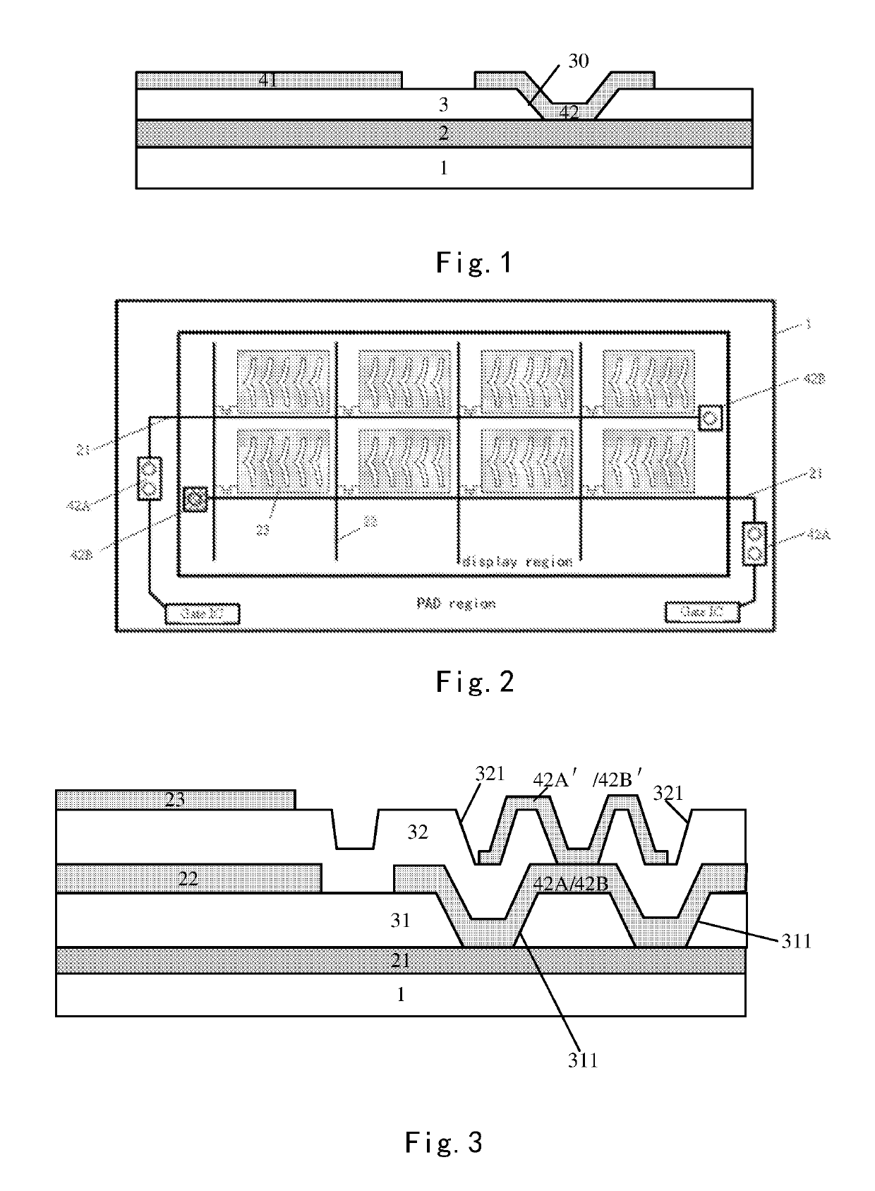
[0029]In an aspect, an embodiment of the present disclosure provides an array substrate. As shown in FIG. 1, the array substrate includes a metal pattern 2 and an electrically conductive pattern 41 formed sequentially on a base substrate 1. The electrically conductive pattern 41 is arranged in a different layer from the layer in which the metal pattern 2 is arranged and is insulated from the metal pattern 2. The array substrate of the present embodiment further includes a static charge releasing pattern 42 formed in a same layer as the electrically conductive pattern...


PUM

PropertyMeasurementUnit
areaaaaaaaaaaa
electrically conductiveaaaaaaaaaa
chargeaaaaaaaaaa

Abstract

An array substrate includes a metal pattern and an electrically conductive pattern formed sequentially on a base substrate. The electrically conductive pattern is insulated from the metal pattern; and a static charge releasing pattern is formed in a same layer as the electrically conductive pattern and formed by a same material as the electrically conductive pattern, the static charge releasing pattern being insulated from the electrically conductive pattern and electrically connected with the metal pattern.

Description

CROSS-REFERENCE TO RELATED APPLICATION[0001]This application is a Section 371 National Stage Application of International Application No. PCT / CN2016 / 094837, filed on Aug. 12, 2016, entitled “ARRAY SUBSTRATE AND METHOD FOR PRODUCING THE SAME” which claims benefit of Chinese Application No. 201610003750.3, filed on Jan. 4, 2016, incorporated herein by reference in their entirety.BACKGROUND OF THE DISCLOSURE[0002]Field of the Disclosure[0003]The present disclosure relates to a field of display, more particularly, to an array substrate and a method for producing the same.[0004]Description of the Related Art[0005]In the conventional process for producing an array substrate, an electrically conductive pattern is typically deposited by plasma glow discharging method. In this way, in the deposition process, more or less electrons will enter the metal pattern that has been formed previously, such that static charge is accumulated in the metal pattern to cause breakdown of adjacent insulated ...

Claims


Application Information

Patent Timeline
Patent Type & Authority Patents(United States)
IPC IPC(8): H01L23/60H01L27/12
CPCH01L27/12H01L23/60H01L27/1244H01L27/1237H01L27/1251H01L27/127H01L27/124H01L27/1259G02F1/136204H01L27/0288
Inventor YANG, XIAOFEIMO, ZAILONGXIN, YANXIADAI, KEZHU, YAWENSU, LEI
Owner BOE TECH GRP CO LTD
Why Eureka
Try Eureka