
High-speed data transfer periods for thyristor memory cell arrays

Active Publication Date: 2020-02-04
TC LAB INC
View PDF2 Cites 0 Cited by
  • Summary
  • Abstract
  • Description
  • Claims
  • Application Information

AI Technical Summary

Benefits of technology

The present invention provides methods for transferring data to and from a memory cell array in a computer chip. The first method allows for quick data transfer by simultaneously reading data from a selected row and latching it in a buffer, before transferring this data to the memory cell array or another buffer. The second method allows for faster data transfer by simultaneously writing a second logic state into the memory cells and latching a second data bit from an external location. These methods relax time constraints and facilitate high-speed data transfer.

Problems solved by technology

Nonetheless, thyristor memory cell arrays have different requirements than DRAMs and under certain circumstances problems may arise.

Method used


Image

  • High-speed data transfer periods for thyristor memory cell arrays
  • High-speed data transfer periods for thyristor memory cell arrays
  • High-speed data transfer periods for thyristor memory cell arrays

Examples


Embodiment Construction

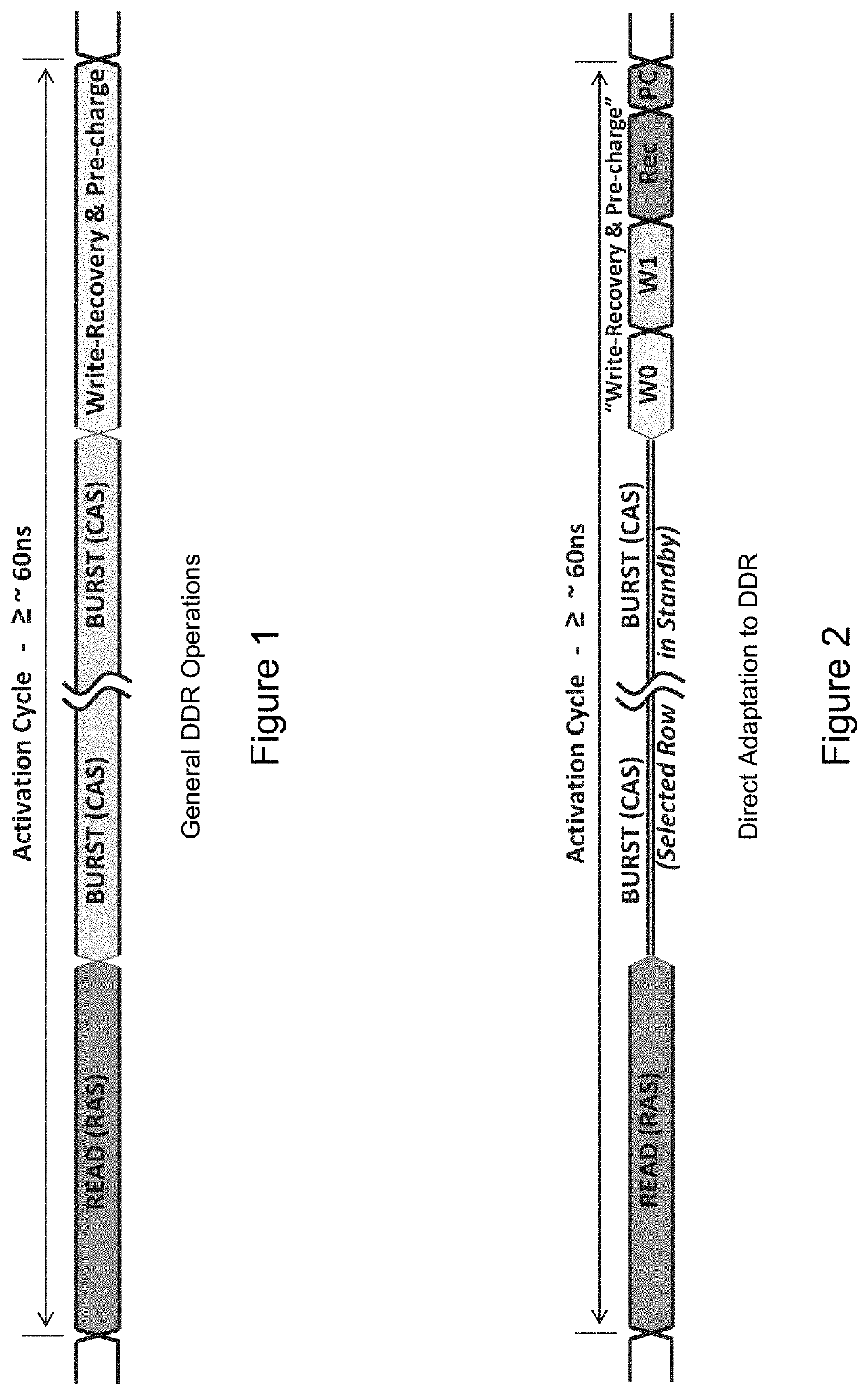
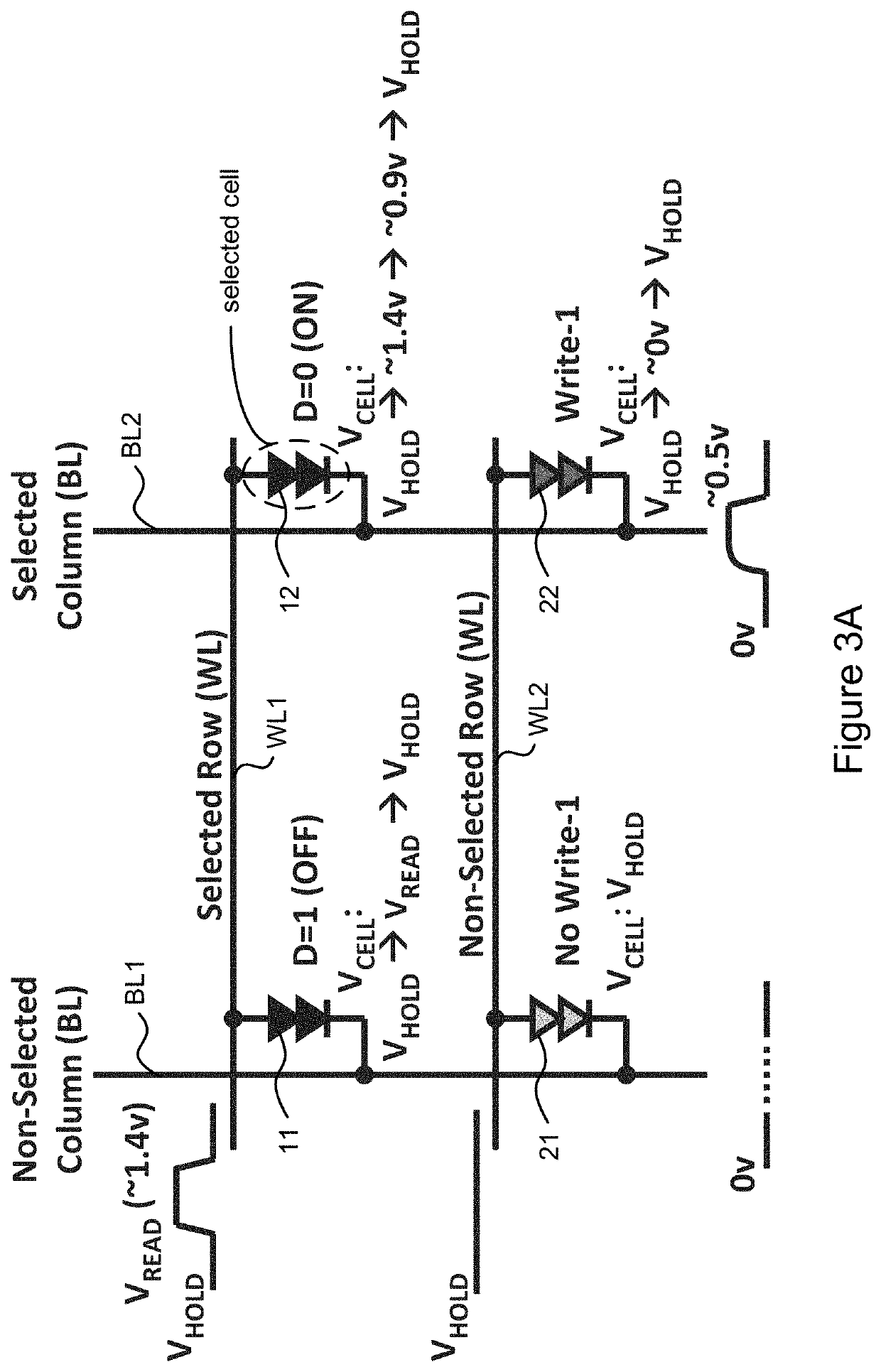
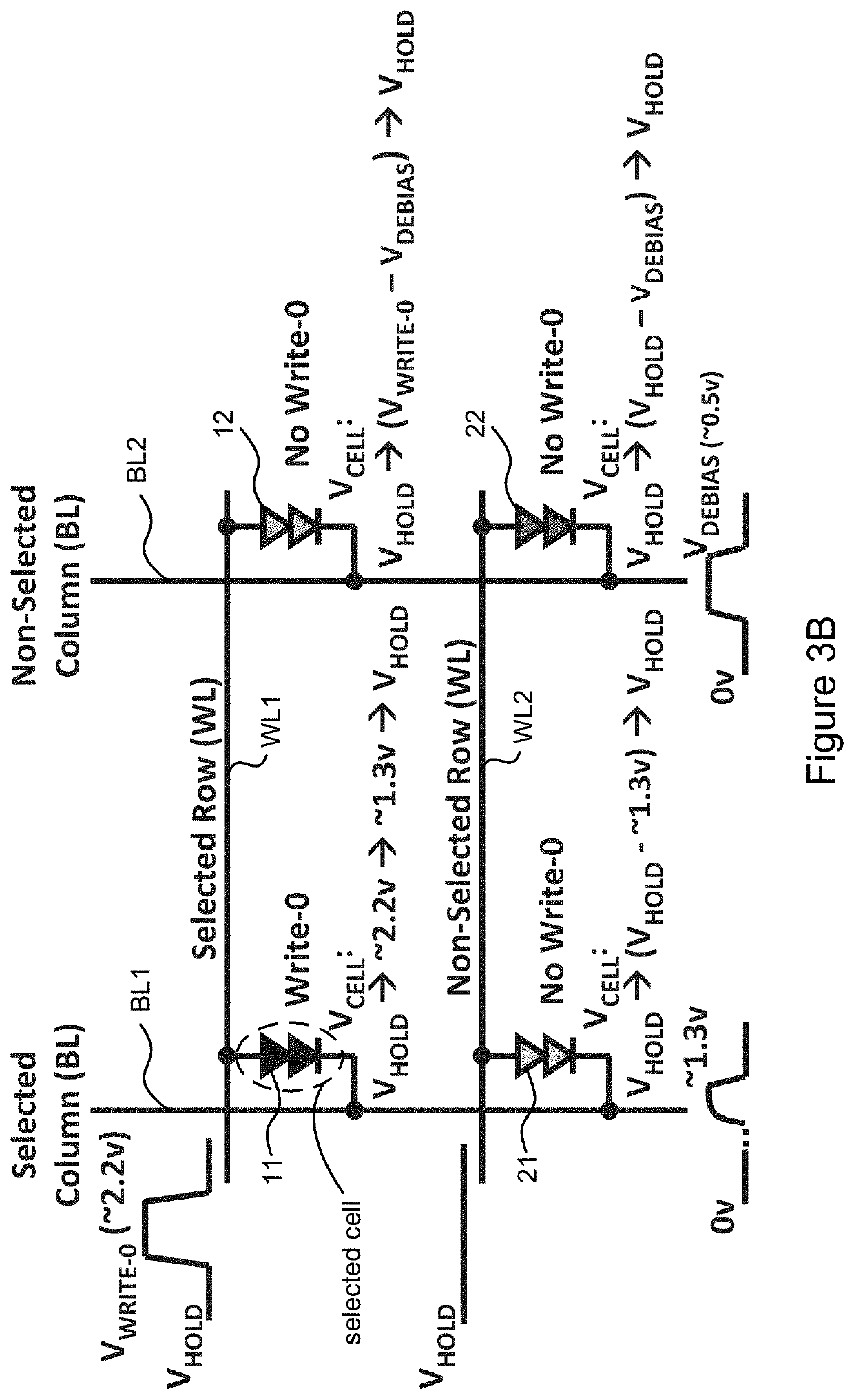
[0018]To best explain the present invention, DDR (DRAMs) is first generally described. This is followed by a direct approach to adapt thyristor memory cell RAMs to DDR constraints for high-speed data transfer. It should be understood that a direct approach does not mean exact imitation of DDR operations since thyristor memory cell RAMs operate differently from DRAMs as will become apparent in the description below. Finally, the present invention is described by which aspects of DDR and thyristor memory cell RAMs are optimally combined for high-speed data transfer.

[0019]Basic Operations and Periods for DDR

[0020]DDR operations are based on an activation cycle in the DRAM array. The cycle starts with a Read operation in which the contents of a selected row (a page) are read and latched. This is followed by a Burst operation in which the latched data is moved to an external location or external data is moved into the DRAM and latched. The data is moved in groups and the bursts can go on...


PUM


Abstract

Aspects of DDR and thyristor memory cell RAMs are optimally combined for high-speed data transfer into and out of RAMs. After a Read operation in which data from a selected row of memory cells in an array are latched, a Burst operation selectively moves the latched data from the array or latches external data. At the same time as the Burst data transfer, all the memory cells of the selected row are turned off or on by a write operation. In the following Write-Back & Pre-charge operation, the latched data bits which are complementary to the memory cell state of the Burst write operation are written back into the corresponding memory cells in the selected row. As part of a DDR-like activation cycle, data can be transferred to and from the memory cell array RAM at high-speed.

Description

CROSS-REFERENCE TO RELATED APPLICATIONS[0001]This patent application claims priority from U.S. Provisional Patent Application No. 62 / 682,103, filed Jun. 7, 2018 and entitled, “High-Speed Transfer of Data To and From Thyristor Memory Cell Arrays,” which is incorporated herein for all purposes.BACKGROUND OF THE INVENTION[0002]Random Access Memory (RAM) is a significant computer system element in which data is stored and retrieved. Heretofore DRAMs (Dynamic Random Access Memories) have constituted most of RAMs. DRAMs are integrated circuits which have the most data packing density with a single memory cell formed by a transistor and a capacitor, often termed 1T1C in abbreviated fashion.[0003]But DRAM technology is nearing its end with the continuing shrinkage of feature dimensions and an emerging technology is thyristor-based memory cell RAMs. At very small dimensions, thyristor memory cell arrays have many advantages over DRAM memory cell arrays, including less power consumption and s...

Claims


Application Information

Patent Timeline
Patent Type & Authority Patents(United States)
IPC IPC(8): G11C11/00G11C11/16G11C13/00
CPCG11C13/0069G11C11/1693G11C11/1675G11C13/004G11C11/1659G11C11/1673G11C13/0004G11C13/003G11C13/0061G11C2213/71G11C11/39G11C11/4076G11C11/408G11C11/409G11C11/4093G11C11/4094G11C2213/35
Inventor BATEMAN, BRUCE L.
Owner TC LAB INC
Learn More