Two-step deposition process

a technology of crystalline materials and deposition processes, which is applied in the manufacture of final products, sustainable manufacturing/processing, electrolytic capacitors, etc., can solve the problems of high risk of human error, non-uniform films or films with pinholes, and high risk of micro-seismic dust on the substrate of spin-coatings, etc., to achieve high purity, high quality, and high quality.

Active Publication Date: 2020-03-03
OXFORD UNIV INNOVATION LTD
View PDF11 Cites 5 Cited by
  • Summary
  • Abstract
  • Description
  • Claims
  • Application Information

AI Technical Summary

Benefits of technology

[0013]Here a new approach to prepare extremely smooth, pinhole-free perovskite (and other crystalline material) films of high purity, for use in photovoltaics and other optical and semiconducting applications is presented. The technique makes use of a two-stage vapour phase technique to ensure extremely high quality of films, with no solution-processing required at all. For instance, initially the metal halide can be deposited via thermal vapour deposition, under high vacuum, to produce a high quality, smooth and pinhole-free film. Subsequently, the film is placed and optionally heated in an atmosphere saturated with the sublimed organic component, causing it to undergo conversion to the perovskite. The advantage of this technique over the previously developed methods is two-fold. Firstly, no solution-processing is required, which enables the most uniform and high quality films to be produced. Secondly, by carrying out the film fabrication in two stages, and depositing the organic at relatively high pressures and relatively low temperatures, it is a much more controlled and reproducible method than the dual source, high vacuum method of Liu, Snaith et al. The process of the invention allows high efficiency perovskite solar cells to be fabricated, and furthermore can enable the fabrication of new perovskite or perovskite-like hybrid materials. The process of the invention circumvents the problems of prior art approaches (for instance Chen et al.) by employing solvent-free vapour deposition approaches. Furthermore, the use of a two-stage vapour process allows materials which have poor solubilities to be used. For instance, the process allows the production of new copper based materials.

Problems solved by technology

However, spin-coating is by its very nature a process which can easily result in non-uniform films or films with pinholes.
Spin-coating is highly susceptible to microscopic amounts of dust on the substrate, precipitates in the solution, local atmosphere composition and temperature, and human error when depositing.
These factors combine to make spin-coating an inherently poorly reproducible process for producing organometal perovskites and other crystalline materials.
Moreover, spin-coating is a process which cannot be easily scaled up.
However, this is a costly process; it requires large quantities of the reagents as well as high temperatures and most importantly, a high vacuum chamber.
Additionally, due to the volatile nature of the organic component employed, it is difficult to control the rate of its deposition, making this process difficult to reproduce between batches.
However, the films produced in this way are substantially non-uniform and the surface of the perovskite layer comprises large crystallites of greater than a micron in size.
The presence of these crystallites causes high surface roughness.
This is likely to be an issue in Willis of reproducibility: if an electrode touches a crystallite of the perovskite penetrating the hole-transport layer it can provide a recombination pathway, lowering device performance and affecting reproducibility.
However, this procedure still makes use of spin-coating to form the metal halide initial film, which results in the aforementioned issues with reproducibility and non-uniformity.
Methods which make use of vacuum evaporation to form the metal halide layer followed by completion of the perovskite by dipping the vacuum evaporated metal halide layer in a solution of the organic component have not succeeded in producing high quality films.
The use of a second solution-based step results in unsuitable perovskite films comprising large crystals and unstable device performance (see Comparative Example 2).

Method used


Image

  • Two-step deposition process
  • Two-step deposition process
  • Two-step deposition process

Examples


example 1

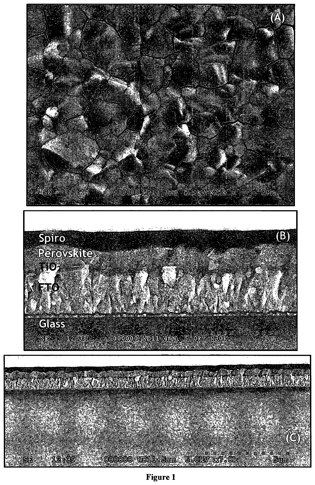
[0254]A photovoltaic device comprising a layer of a methylammonium lead iodide perovskite was produced by the following procedure which includes the two-step vapour / vapour deposition method according to the invention. FTO glass was first cleaned before being spin-coated with an electron selective layer of TiO2 having a thickness of approximately 50 nm. A layer of lead diiodide (PbI2) was then evaporated onto the electron selective layer at a pressure of approximately 5×10⁻⁶ mbar and a rate of 0.2 nm / s until a layer of PbI2 having a thickness of from 250 to 300 nm was formed. The sample comprising the PbI2 layer was then transferred through a lab atmosphere to a nitrogen filled glovebox. The sample was put in a covered glass container at atmospheric pressure together with methylammonium iodide (MAI, CH3NH3I) and the container was heated to 150° C. The substrate and the MAI powder were held at the same temperature for 2 hours. The PbI2 layer was converted to methylammonium lead iodide...

example 2

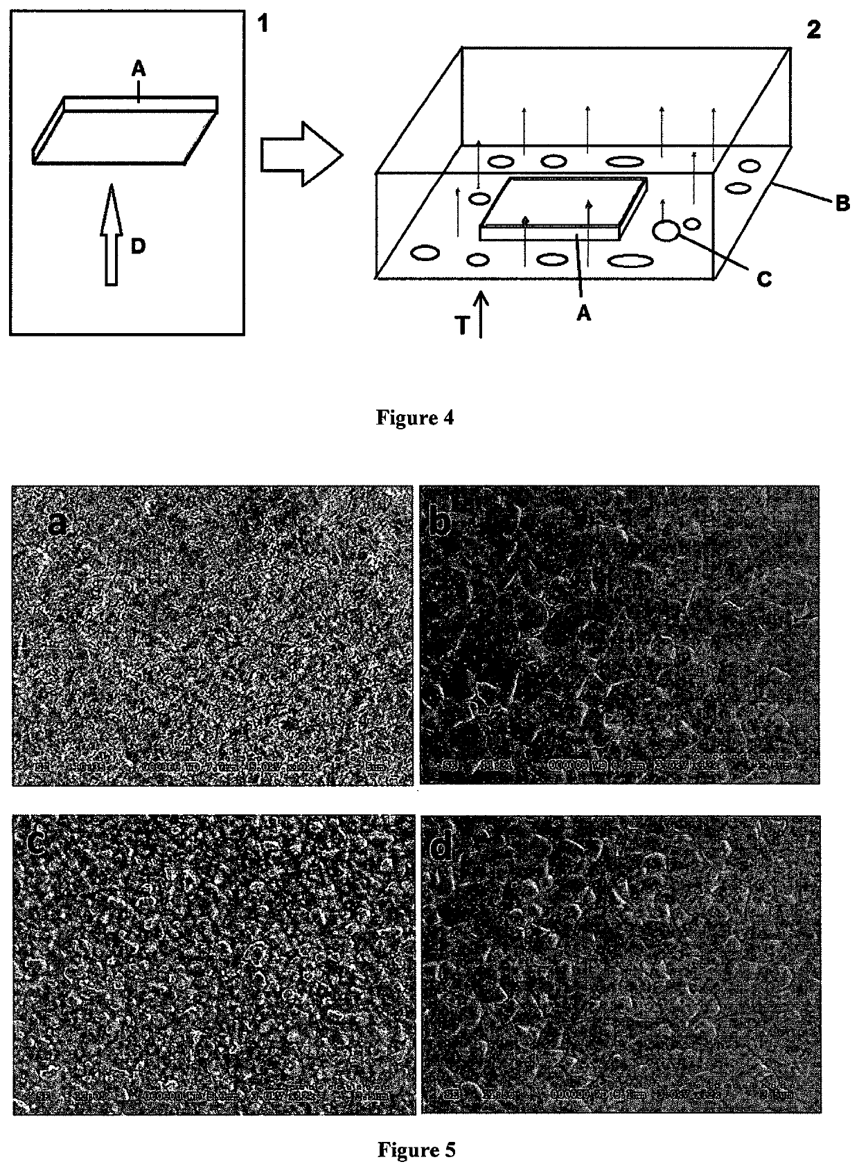
[0258]Layers of lead iodide (PbI2) were produced by either spin-coating a solution comprising PbI2 (comparative) or by vacuum evaporating PbI2 at a pressure of approximately 5×10⁻⁶ mbar (the invention). These layers were then exposed to a sublimed vapour of methylammonium iodide (MAI) at approximately atmospheric pressure for 90 minutes by placing the PbI2 layers in a heated sealed container with MAI powder. FIG. 5 shows SEM images of top-views of the produced layers. FIG. 5(a) shows a top-view SEM of a spin-coated PbI2 surface. FIG. 5(b) shows a top-view SEM of a methylammonium lead triiodide surface produced by exposing the spin-coated PbI2 surface of FIG. 5(a) to the vapour of MAI. FIG. 5(c) shows a top-view SEM of an evaporated PbI2 surface. FIG. 5(d) shows a top-view SEM of a methylammonium lead triiodide surface produced by exposing the evaporated PbI2 surface of FIG. 5(c) to the vapour of MAI.

[0259]The conversion of the spin-coated layer of PbI2 to CH3NH3PbI3 can be seen in F...

example 3

[0262]A two-step process was used to produce other perovskite materials. Methylammonium tin iodide was produced by converting a spin-coated layer of tin iodide in a methylammonium iodide (MAI) atmosphere. The partial conversion of the layer of SnI2 to CH3NH3SnI3 is shown in FIG. 10 which shows the XRD patter of SnI2 alone and after 15 exposure to an MAI atmosphere. Perovskite peaks are marked with a *.

[0263]FIGS. 11, 12 and 13 show XRD patterns of copper based materials produced using a spin-coated metal halide / vapour deposited organic method. Exposure to the atmosphere of the nitrogen containing component was for approximately 90 minutes. FIG. 11 shows the XRD of a perovskite produced by exposing a spin-coated layer of CuBr2 to an atmosphere of methylammonium chloride. FIG. 12 shows the XRD of a perovskite produced by exposing a spin-coated layer of CuCl2 to an atmosphere of methylammonium chloride. FIG. 13 shows the XRD of a perovskite produced by exposing a spin-coated layer of C...


PUM

PropertyMeasurementUnit
pressureaaaaaaaaaa
pressureaaaaaaaaaa
temperatureaaaaaaaaaa

Abstract

The present invention provides a process for producing a layer of a crystalline material comprising a perovskite or a hexahalometallate, which process comprises: (i) exposing a substrate to a vapour comprising a first precursor compound in a first chamber to produce a layer of the first precursor compound on the substrate; and (ii) exposing the layer of the first precursor compound to a vapour comprising a second precursor compound in a second chamber to produce the layer of a crystalline material, wherein the pressure in the second chamber is above high vacuum. The invention also provides a process for producing a layer of a crystalline material comprising a perovskite or a hexahalometallate, which process comprises exposing a layer of a first precursor compound on a substrate to a vapour comprising a second precursor compound in a chamber to produce the layer of a crystalline material, wherein the pressure in the chamber is greater than high vacuum and less than atmospheric pressure. The invention also provides a process for producing a semiconductor device comprising a layer of a crystalline material, which process comprises producing said layer of a crystalline material by a process as according to the invention.

Description

CROSS-REFERENCE TO RELATED APPLICATIONS[0001]This application represents the national stage entry of PCT International Application No. PCT / GB2015 / 051993 filed Jul. 9, 2015 and claims priority to Great Britain Patent Application No. 1412201.4 filed on Jul. 9, 2014. The contents of this application are hereby incorporated by reference as if set forth in their entirety herein.FIELD OF THE INVENTION[0002]The present invention relates to a process for producing a layer of a crystalline material. A process for producing a semiconductor device comprising a layer of a crystalline material is also described.[0003]The work leading to this invention has received funding from the European Community's Seventh Framework Programme (FP7 / 2007-2013) under grant agreement no. 279881.BACKGROUND OF THE INVENTION[0004]Hybrid organic-inorganic perovskite materials have recently become a topic of extreme interest for photovoltaics, with devices based on these materials now reaching power conversion efficie...

Claims


Application Information

Patent Timeline
Patent Type & Authority Patents(United States)
IPC IPC(8): H01L21/00C23C14/06C23C14/12C23C14/58C23C14/00C23C16/455H01L51/42H01G9/20C23C14/24C23C16/40H01L51/00H01L31/0256
CPCC23C14/5846C23C14/24H01L51/422C23C14/5893H01L51/0077H01G9/2027C23C14/0021H01L51/0002H01L51/006C23C16/409H01L51/0032C23C16/45553C23C14/0694H01G9/2009C23C14/12C23C16/45557H01L2031/0344Y02E10/549H01L51/0056H01L2251/306H01L51/4226Y02P70/521Y02E10/542Y02P70/50H10K85/00H10K85/633H10K30/151H10K2102/102H10K85/50C23C14/5806C23C14/54H01L33/0008H01L31/10H01L31/036H01L31/18H10K71/10H10K85/30H10K30/15H10K85/624
Inventor SNAITH, HENRY J.EPERON, GILES E.BALL, JAMES M.
Owner OXFORD UNIV INNOVATION LTD
Why Eureka
Try Eureka