
Circuit board and manufacturing method thereof

a technology of circuit boards and manufacturing methods, applied in the field of circuit boards, can solve the problems of reducing the yield in the manufacturing process of circuit boards, and achieve the effect of reducing the yield

Active Publication Date: 2020-04-07
FANUC LTD
View PDF9 Cites 0 Cited by
  • Summary
  • Abstract
  • Description
  • Claims
  • Application Information

AI Technical Summary

Benefits of technology

The present invention aims to provide a circuit board that can reduce a decrease in yield, detect degradation, and method of manufacturing it. The technical effects of the invention include reducing the likelihood of failures in the manufacturing process, improving reliability and performance of the circuit board, and reducing costs associated with manufacturing.

Problems solved by technology

However, the pattern whose width is narrower than the other wiring patterns or the pattern whose insulation distance is shorter than them is present, and thus the yield in the manufacturing process of the circuit board is decreased.

Method used


Image

  • Circuit board and manufacturing method thereof
  • Circuit board and manufacturing method thereof
  • Circuit board and manufacturing method thereof

Examples


first embodiment

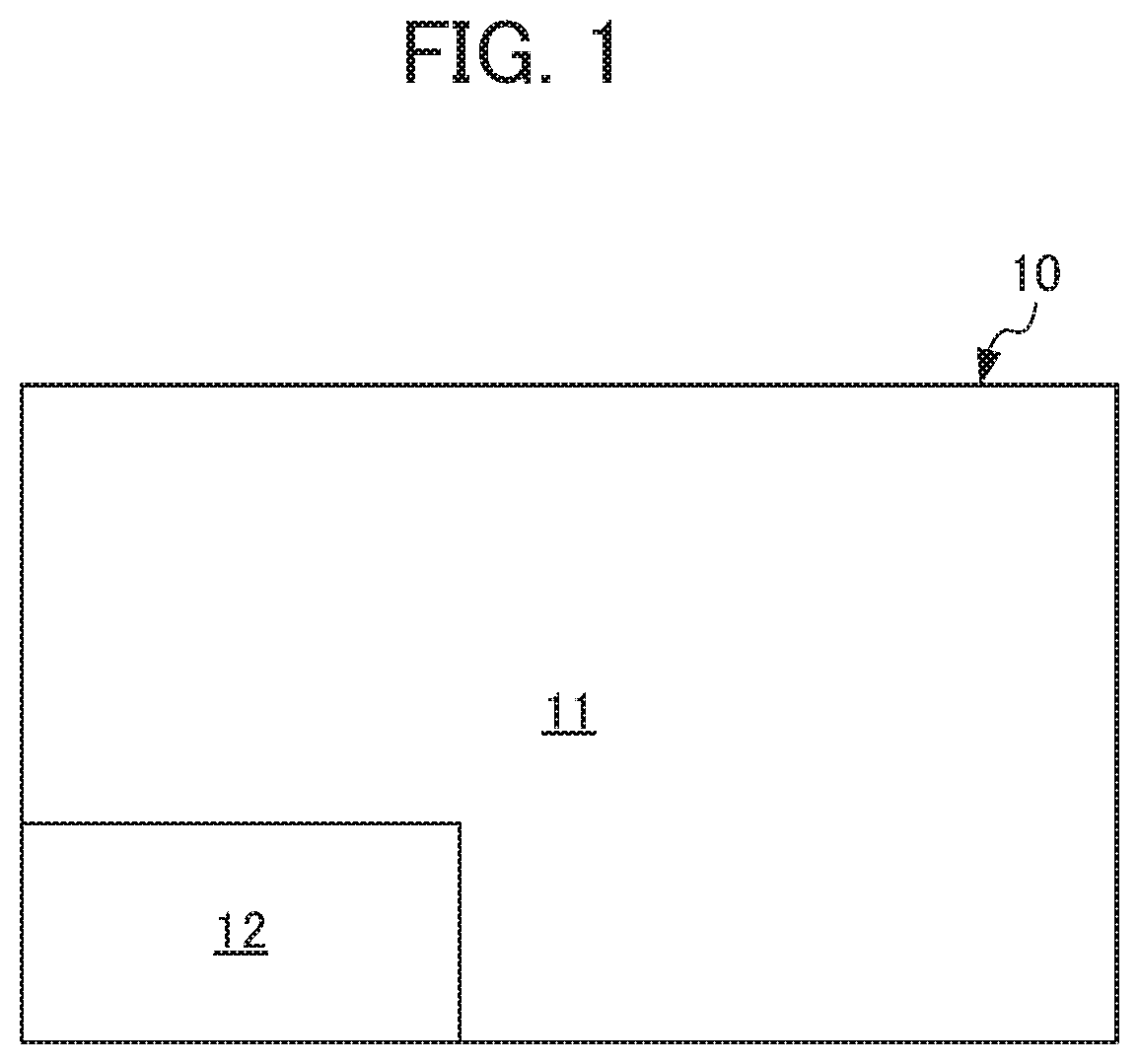
[0019]A circuit board 10 according to the first embodiment will first be described with reference to FIG. 1. FIG. 1 is a plan view of the circuit board 10.

[0020]As shown in FIG. 1, the circuit board 10 is obtained by providing a wiring pattern on an insulating board, and is applied to a machine tool, a robot controller and the like. The circuit board 10 includes a first region 11 and a second region 12.

[0021]In the first region 11, a first wiring pattern is provided on which a first surface treatment is applied. Examples of the first surface treatment include solder coat and Au flash.

[0022]In the second region 12, a second wiring pattern is provided on which a second surface treatment having a cutting fluid resistance lower than the first surface treatment is applied. The second region 12 includes a corner portion of the circuit board 10. Examples of the second surface treatment include pre-flux, Sn plating and Ag plating. Examples of the cutting fluid include a liquid containing ch...

second embodiment

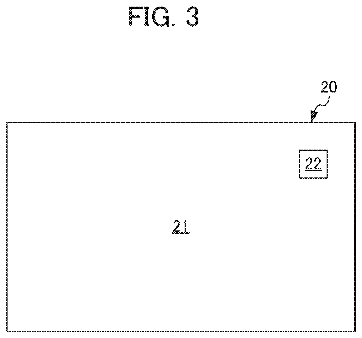
[0031]A circuit board 20 according to the second embodiment will then be described with reference to FIGS. 3 and 4. FIG. 3 is a plan view of the circuit board 20. FIG. 4 is a side cross-sectional view of the circuit board 20 shown in FIG. 3.

[0032]As shown in FIGS. 3 and 4, the circuit board 20 includes a first circuit board 21, a second circuit board 22, a pad 23 and a solder joint portion 24.

[0033]The first circuit board 21 is obtained by providing, on a first insulating board, a first wiring pattern on which a first surface treatment is applied. The first surface treatment in the second embodiment is the same as that in the first embodiment. On the first circuit board 21, the first surface treatment is totally applied. The outside shape of the first circuit board 21 agrees with the outside shape of the circuit board 20 in plan view.

[0034]The second circuit board 22 is obtained by providing, on a second insulating board, a second wiring pattern on which a second surface treatment i...


PUM


Abstract

A circuit board is obtained by providing a wiring pattern on an insulating board. The circuit board includes a first region and a second region. In the first region, a first wiring pattern is provided on which a first surface treatment is applied. In the second region, a second wiring pattern is provided on which a second surface treatment having a cutting fluid resistance and / or a humidity resistance lower than the first surface treatment is applied.

Description

[0001]This application is based on and claims the benefit of priority from Japanese Patent Application No. 2018-037907, filed on Mar. 2, 2018, the content of which is incorporated herein by reference.BACKGROUND OF THE INVENTIONField of the Invention[0002]The present invention relates to a circuit board and a method of manufacturing it.Related Art[0003]Conventionally, under an environment in which a machine tool is used, a cutting fluid is converted into mist so as to be adhered to a circuit board within an electrical / electronic device. Hence, a wiring pattern is corroded (electrolytically corroded) so as to be broken, and thus a failure occurs in the device. The cause of electrolytic corrosion of a wiring pattern is not limited to a cutting fluid, and the electrolytic corrosion may be caused by humidity (water). In order to prevent the failure caused by the electrolytic corrosion or the corrosion of the wiring pattern as described above, various methods of detecting degradation of a...

Claims


Application Information

Patent Timeline
Patent Type & Authority Patents(United States)
IPC IPC(8): H05K1/09H05K3/00H05K3/26H05K1/11
CPCH05K3/26H05K1/111H05K1/09H05K3/0097H05K2201/0776H05K1/0266H05K3/22H05K3/244H05K2201/10151H05K2203/1173
Inventor SAIDO, NORIHIRO
Owner FANUC LTD
Learn More