Semiconductor memory device error correction circuit, semiconductor memory device including the same, and memory system including the same

a technology of error correction circuit and memory device, which is applied in the field of memory devices, can solve the problems of reducing the yield of dram devices and increasing the bit errors of memory cells in dram devices, and achieve the effect of improving performance and reliability in error correction

Active Publication Date: 2020-04-28
SAMSUNG ELECTRONICS CO LTD
View PDF21 Cites 3 Cited by
  • Summary
  • Abstract
  • Description
  • Claims
  • Application Information

AI Technical Summary

Benefits of technology

[0004]Exemplary embodiments of the present disclosure provide an error correction circuit of a semiconductor memory device capable of improving performance and reliability, a semiconductor memory device including the same, and a memory system including the same.
[0009]According to exemplary embodiments of the present disclosure, an ECC is represented by a generation matrix, includes a plurality of column vectors, and the column vectors are divided into first through fourth code groups corresponding to the first through fourth sub codeword groups, respectively. The column vectors have elements configured to restrict a location of a sub codeword group in which a miscorrected bit occurs, in which the miscorrected bit is generated by error bits of the main data. As a result, performance and reliability relating to error correction may be improved.

Problems solved by technology

Due to the continuing reduction in fabrication design rules of DRAM devices, bit errors of memory cells in DRAM devices may increase, and the yield of DRAM devices may decrease.

Method used


Image

  • Semiconductor memory device error correction circuit, semiconductor memory device including the same, and memory system including the same
  • Semiconductor memory device error correction circuit, semiconductor memory device including the same, and memory system including the same
  • Semiconductor memory device error correction circuit, semiconductor memory device including the same, and memory system including the same

Examples


Embodiment Construction

[0036]Exemplary embodiments of the present disclosure will be described more fully hereinafter with reference to the accompanying drawings. Like reference numerals may refer to like elements throughout the accompanying drawings.

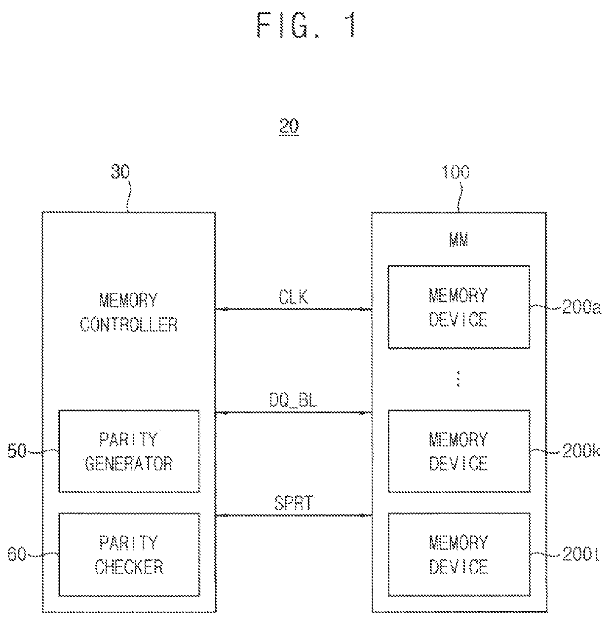
[0037]FIG. 1 is a block diagram illustrating a memory system according to exemplary embodiments of the present disclosure.

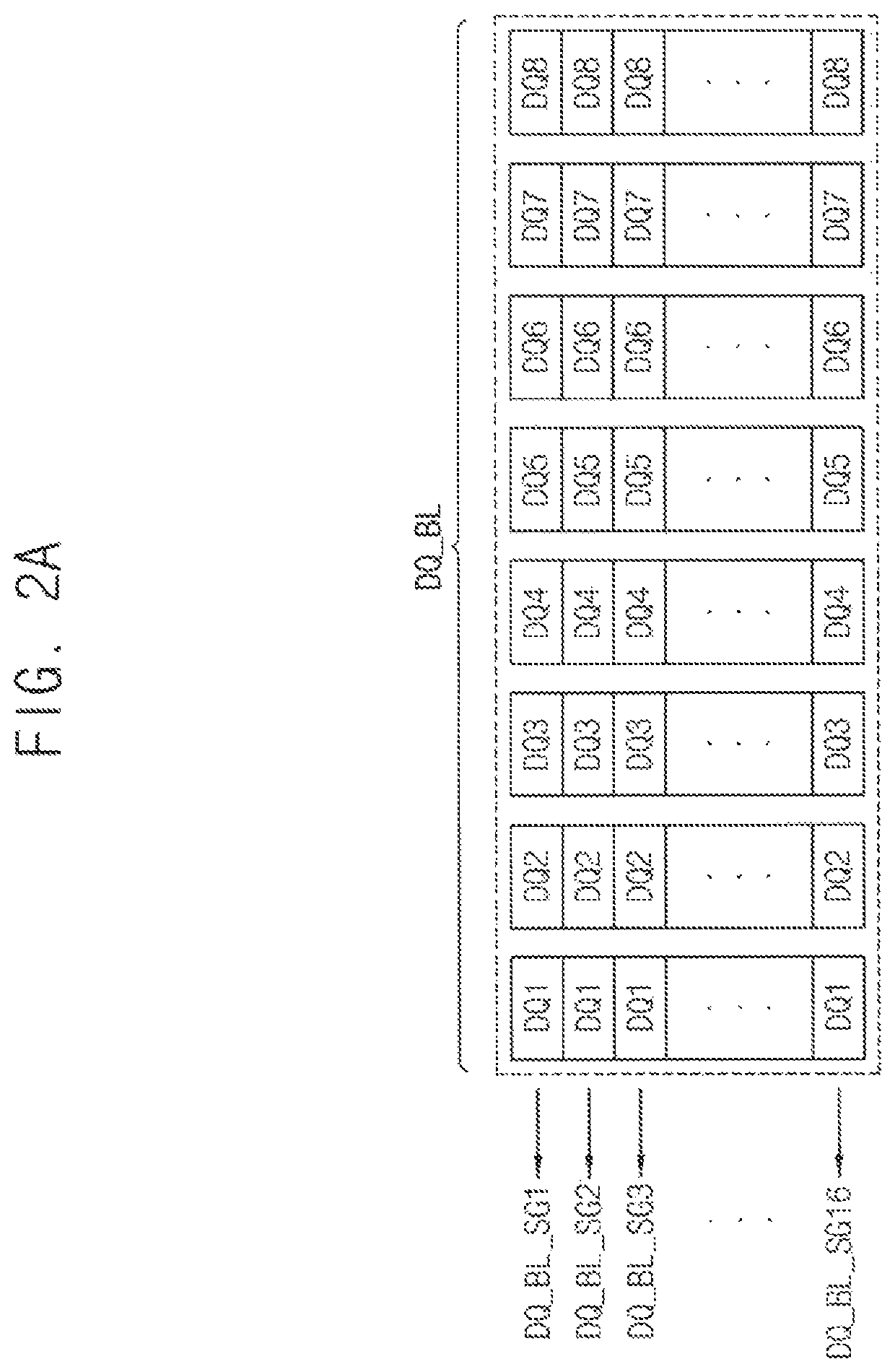
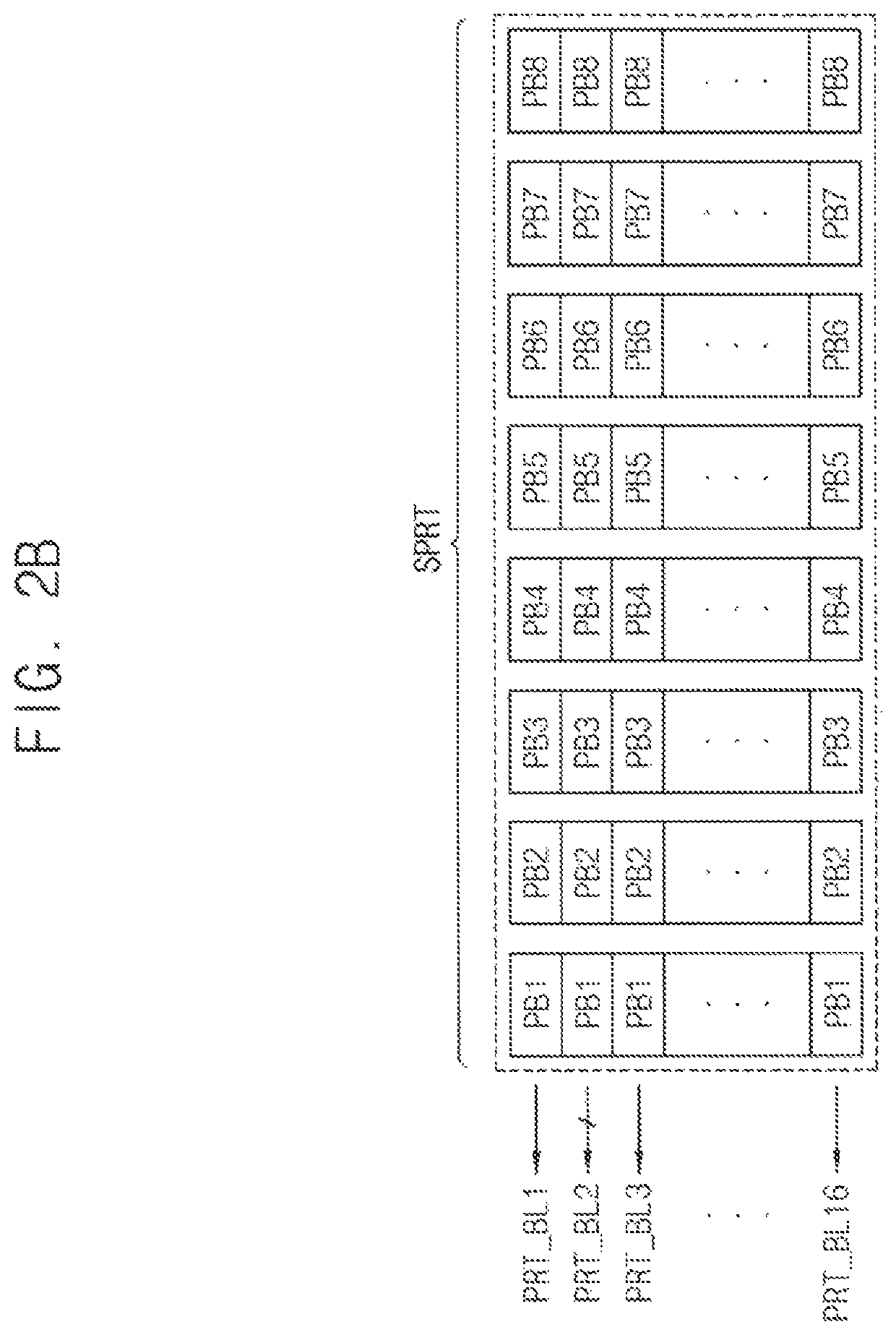
[0038]Referring to FIG. 1, a memory system 20 may include a memory controller 30 and a memory module 100. The memory module 100 includes a plurality of memory devices 200a˜200k and 200t. The plurality of memory devices 200a˜200k and 200t includes a plurality of data memories 200a˜200k and a 200t.

[0039]The memory controller 30 may control an overall operation of the memory system 20. The memory controller 30 may control an overall data exchange between a host and the plurality of memory devices 200a˜200k and 200t. For example, the memory controller 30 may write data in the plurality of memory devices 200a˜200k and 200t or read data from th...


PUM


Abstract

An error correction circuit of a semiconductor memory device including a memory cell array includes an error correction code (ECC) memory that stores an ECC and an ECC engine. The ECC is represented by a generation matrix. The ECC engine generates first parity data based on main data using the ECC, and corrects at least one error bit in the main data read from the memory cell array using the first parity data. The main data includes a plurality of data bits divided into a plurality of sub codeword groups. The ECC includes a plurality of column vectors divided into a plurality of code groups corresponding to the sub codeword groups. The column vectors have elements configured to restrict a location of a sub codeword group in which a mis-corrected bit occurs, in which the mis-corrected bit is generated due to error bits in the main data.

Description

CROSS-REFERENCE TO RELATED APPLICATIONS[0001]This application claims priority under 35 U.S.C. § 119 to Korean Patent Application No. 10-2017-0085809, filed on Jul. 6, 2017, the disclosure of which is incorporated by reference herein in its entirety.TECHNICAL FIELD[0002]Exemplary embodiments of the present disclosure relate to memory devices, and more particularly, to error correction circuits of semiconductor memory devices, semiconductor memory devices including the same, and memory systems including the same.DISCUSSION OF THE RELATED ART[0003]Semiconductor memory devices may be classified as non-volatile memory devices, such as flash memory devices, and volatile memory devices, such as dynamic random access memory (DRAM) devices. DRAM devices are often used for system memories due to their high speed operation and cost efficiency. Due to the continuing reduction in fabrication design rules of DRAM devices, bit errors of memory cells in DRAM devices may increase, and the yield of D...

Claims


Application Information

Patent Timeline
Patent Type & Authority Patents(United States)
IPC IPC(8): G06F11/10G11C29/52G11C29/00G11C29/04
CPCG06F11/1068G11C29/52G11C29/72G06F11/1048G11C2029/0409G11C2029/0411G11C29/42Y02D10/00G06F11/1008
Inventor CHA, SANG-UHNKIM, MYEONG-O
Owner SAMSUNG ELECTRONICS CO LTD
Why Eureka
Try Eureka