Conductive member and touch panel
a touch panel and conductive technology, applied in the field of conductive members, can solve the problems of decreased visibility, increased distance between adjacent metal thin wires, and increased visibility, and achieve the effects of suppressing the generation of moires, high detection sensitivity, and improved visibility
- Summary
- Abstract
- Description
- Claims
- Application Information
AI Technical Summary
Benefits of technology
Problems solved by technology
Method used
Image

Examples
embodiment 1
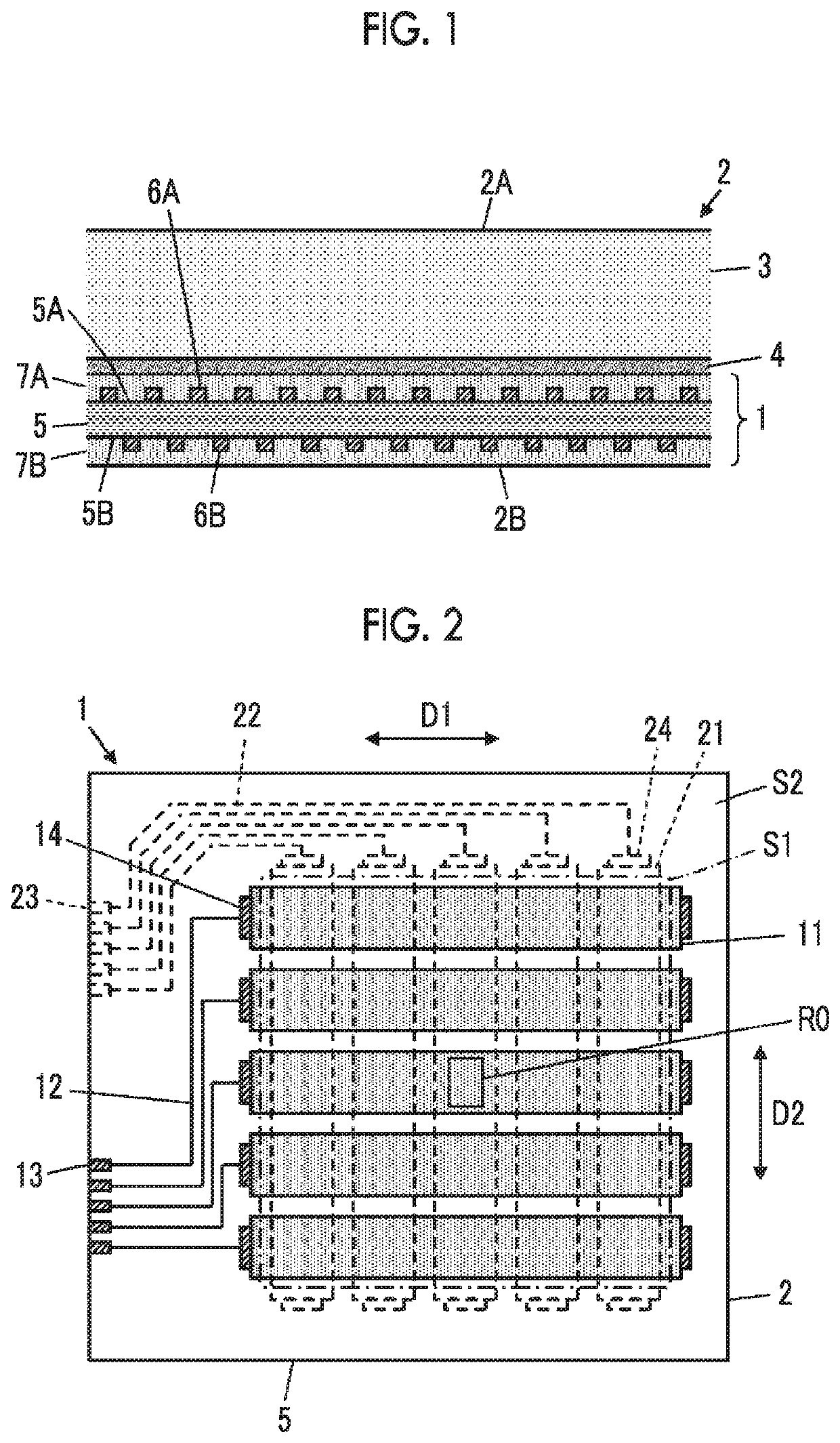
[0061]FIG. 1 illustrates a configuration of a touch panel 2 in which a conductive member 1 according to Embodiment 1 of the present invention is used.
[0062]The touch panel 2 has a front surface 2A and a back surface 2B, and is used in a state in which a display device (not illustrated) such as a liquid crystal display device is arranged on the back surface 2B side. The front surface 2A of the touch panel 2 is a touch detection surface, and becomes a viewing side on which an operator of the touch panel 2 observes an image of the display device through the touch panel 2.
[0063]The touch panel 2 has a transparent insulating cover panel 3 having a flat plate shape, which is arranged on the front surface 2A, and the conductive member 1 is bonded to a surface of the cover panel 3 opposite to the front surface 2A via a transparent adhesive 4.
[0064]In the conductive member 1, metal fine wires 6A and metal fine wires 6B are respectively formed on both surfaces of a transparent insulating subs...
embodiment 2
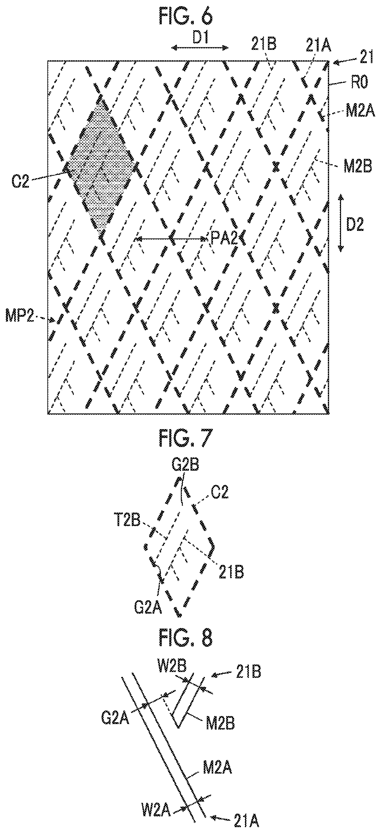
[0132]In Embodiment 1 described above, the dummy pattern portions 11B in the first electrode having the first dummy unit pattern T1B illustrated in FIG. 4 are arranged inside each mesh of the first mesh pattern MP1 formed of the first detection electrode portions 11A, and the dummy pattern portions 21B in the second electrode having the second dummy unit pattern T2B illustrated in FIG. 7 are arranged inside each mesh of the second mesh pattern MP2 formed of the second detection electrode portions 21A, but the first dummy unit pattern T1B and the second dummy unit pattern T2B are not limited to those illustrated in FIGS. 4 and 7.
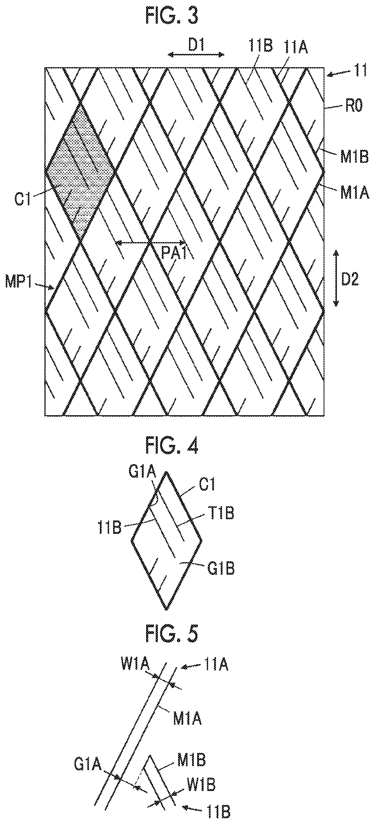
[0133]FIG. 10 illustrates a partial plan view of only a first electrode 31 in an electrode intersection portion of a conductive member according to Embodiment 2 seen from a viewing side. The first electrode 31 is formed on the first surface 5A of the transparent insulating substrate 5 illustrated in FIG. 1.
[0134]The first electrode 31 has first detection elec...
embodiment 3
[0146]FIG. 15 illustrates a partial plan view of only a first electrode 51 in an electrode intersection portion of a conductive member according to Embodiment 3 seen from a viewing side. The first electrode 51 is formed on the first surface 5A of the transparent insulating substrate 5 illustrated in FIG. 1.
[0147]The first electrode 51 has first detection electrode portions 51A which are drawn by relatively thick lines in FIG. 15 and dummy pattern portions 51B in the first electrode which are drawn by relatively thin lines in FIG. 15. The first detection electrode portions 51A and the dummy pattern portions 51B in the first electrode are respectively formed of the metal fine wires M1A and the metal fine wires M1B, and the dummy pattern portions 51B in the first electrode are arranged so as to be not electrically connected to the first detection electrode portions 51A and insulated from the first detection electrode portions 51A.
[0148]In the same manner as the first detection electrod...
PUM
| Property | Measurement | Unit |
|---|---|---|
| light transmittance | aaaaa | aaaaa |
| light transmittance | aaaaa | aaaaa |
| light transmittance | aaaaa | aaaaa |
Abstract
Description
Claims
Application Information
 - R&D
- Intellectual Property
- Life Sciences
- Materials
- Tech Scout
- Unparalleled Data Quality
- Higher Quality Content
- 60% Fewer Hallucinations
Browse by: Latest US Patents, China's latest patents, Technical Efficacy Thesaurus, Application Domain, Technology Topic, Popular Technical Reports.
© 2025 PatSnap. All rights reserved.Legal|Privacy policy|Modern Slavery Act Transparency Statement|Sitemap|About US| Contact US: help@patsnap.com