Organic light emitting diode device and manufacturing method thereof

a light-emitting diode and organic technology, applied in the field of display, can solve the problems of increasing mechanical unreliability, affecting the actual display area, and consuming about 90% of current full-screen products, so as to reduce fragility, increase the integration degree of the display panel, and increase the display area

Active Publication Date: 2020-11-24
WUHAN CHINA STAR OPTOELECTRONICS SEMICON DISPLAY TECH CO LTD
View PDF4 Cites 0 Cited by
  • Summary
  • Abstract
  • Description
  • Claims
  • Application Information

AI Technical Summary

Benefits of technology

[0005]The present disclosure provides an organic light emitting diode (OLED) device and a manufacturing method thereof, which can solve a black border caused by COF / COP, and increase an effective display area of the display panel, and enhance the mechanical strength of the DIC / touch integrated circuit (TIC).
[0053]The benefits of the present disclosure are: compared to existing OLED devices, the OLED device and the manufacturing method thereof of the present disclosure introduce signals of the thin film transistor layer, the pixel unit layer and the touch layer onto an independent signal layer by using a via method, and after bonding the first driving chip (DIC), the flexible circuit board (FPC) can be directly disposed under the display panel without bending to eliminate a black border caused by COF / COP and effectively increase the display area. Meanwhile, by adding a protective buffer layer under the first driving chip and the second driving chip (TIC), the FPC of the first driving chip and the second driving chip is integrated, thereby increasing the integration degree of the display panel; the first driving chip / second driving chip is protected by the high-viscosity opaque adhesive, which can reduce the fragility and enhance the mechanical strength; since pins of the first driving chip / the second driving chip are protected by a high viscosity opaque adhesive, it is difficult to analyze optical, electrical and other properties by conventional means, such as a light mirror, an oscilloscope, a multimeter, etc., and enhance the data confidentiality thereof.

Problems solved by technology

However, due to the problems of the existing panel design and manufacturing process, such as positions of a headphone, a front camera, a fingerprint recognition, an iris recognition element, etc., will occupy a part of the display area, so the current full screen product may consumes about 90%.
Due to the problem of minimum bending radius of the PI or film material, it will inevitably leave some borders in a bending area and affect the actual display area.
Moreover, the presence of the bending area does not only increase the mechanical unreliability but also requires some special design for high-speed signal transmission.

Method used


Image

  • Organic light emitting diode device and manufacturing method thereof
  • Organic light emitting diode device and manufacturing method thereof

Examples


Embodiment Construction

[0059]The following descriptions for the respective embodiments are specific embodiments capable of being implemented for illustrations of the present disclosure with referring to appended figures. The terms of up, down, front, rear, left, right, interior, exterior, side, etcetera are merely directions of referring to appended figures. Thus, the used directional terms are used to describe and understand the present disclosure, but the present disclosure is not limited thereto. In the figure, units with similar structures are denoted by the same reference numerals.

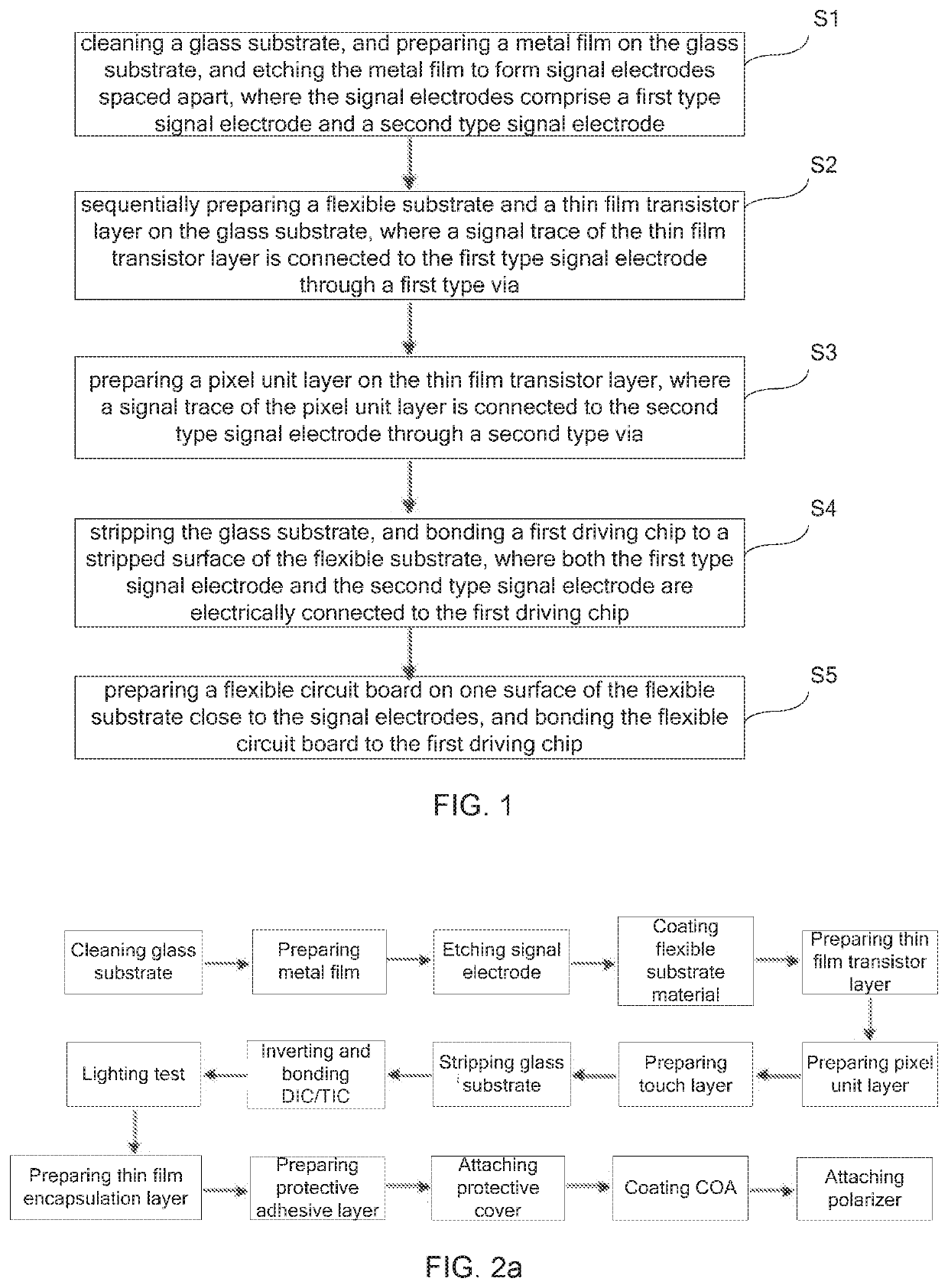
[0060]The OLED device of the prior art is influenced by the bending property of the COF / COP material, and leaves a black border on the bonding area of the display panel, thereby affecting the actual display area of the display panel. Meanwhile, the presence of the bonding area also increases the technical problems of mechanical unreliability. This embodiment can solve the defects.

[0061]As shown in FIG. 1, a flow chart of a ...


PUM

PropertyMeasurementUnit
flexibleaaaaaaaaaa
viscosityaaaaaaaaaa
display areaaaaaaaaaaa

Abstract

Provided is an OLED device and a manufacturing method thereof. The OLED device includes: a flexible substrate having signal electrodes embedded on a surface of one side of the flexible substrate and a thin film transistor layer and a pixel unit layer prepared on a surface of the other side; both a first driving chip and a flexible circuit board are disposed on a back surface of the flexible substrate; signal traces in the thin film transistor layer and the pixel unit layer are connected to corresponding signal electrodes through vias, and the signal electrodes are connected to the first driving chip.

Description

RELATED APPLICATIONS[0001]This application is a National Phase of PCT Patent Application No. PCT / CN2018 / 104970 having International filing date of Sep. 11, 2018, which claims the benefit of priority of Chinese Patent Application No. 201810907178.2 filed on Aug. 10, 2018. The contents of the above applications are all incorporated by reference as if fully set forth herein in their entirety.FIELD AND BACKGROUND OF THE INVENTION[0002]The present disclosure relates to a display field, and more particularly to an organic light emitting diode device and a manufacturing method thereof.[0003]With the releases of full screen phones, such as Samsung S8 / Note 8 and iPhone X, the full screen technology is now the trend. The full screen means that a front of a mobile phone is all used to display effective information. The surrounding of the mobile phone is designed without borders for pursuing a screen ratio close to 100%. Thus, a display area of the mobile phone is greatly improved. The beauty o...

Claims


Application Information

Patent Timeline
Patent Type & Authority Patents(United States)
IPC IPC(8): H01L51/00H01L51/56H01L51/52G06F3/041H01L27/32
CPCH01L27/3276H01L51/5281H01L51/56H01L51/5253G06F3/0412H01L51/003H01L27/323H01L51/0031H01L51/0097H01L2227/326H01L2251/5338G06F2203/04102G06F2203/04103H10K59/12H10K59/131H10K59/1201Y02E10/549Y02P70/50H10K59/40H10K71/80H10K77/111H10K50/86H10K50/844H10K71/00H10K71/70H10K2102/311
Inventor WANG, HAIYAN, WEINANTSAI, KUNYUEH
Owner WUHAN CHINA STAR OPTOELECTRONICS SEMICON DISPLAY TECH CO LTD
Why Eureka
Try Eureka