Semiconductor light emitting element

a technology of light-emitting elements and semiconductors, applied in the direction of basic electric elements, semiconductor devices, electrical equipment, etc., can solve the problems of uneven current density distribution, achieve the effects of reducing forward voltage, light-emitting output, and reducing in-plane uneven current density distribution

Active Publication Date: 2021-01-26
NICHIA CORP
View PDF27 Cites 1 Cited by
  • Summary
  • Abstract
  • Description
  • Claims
  • Application Information

AI Technical Summary

Benefits of technology

[0005]Certain embodiments of the present disclosure allow for obtaining a semiconductor light emitting element in which light emission output can be improved while reducing a forward voltage, and unevenness of a current density distribution can be reduced.
[0007]According to certain embodiments of the present disclosure, light emission output can be improved while reducing a forward voltage, and in-plane unevenness of a current density distribution can be reduced.

Problems solved by technology

In addition, some arrangement patterns of a plurality of n-contact portions in a top view of the semiconductor layered body may cause unevenness in current density distribution.

Method used


Image

  • Semiconductor light emitting element
  • Semiconductor light emitting element
  • Semiconductor light emitting element

Examples


first embodiment

[0028]Configuration of Semiconductor Light Emitting Element

[0029]A configuration of a semiconductor light emitting element according to a first embodiment of the present disclosure will be described with reference to FIGS. 1 to 10. The plan views of FIGS. 8 to 10 schematically illustrate states during manufacturing, which correspond to the sectional views of FIGS. 12 to 14 showing a process of manufacturing a semiconductor light emitting element 100, respectively.

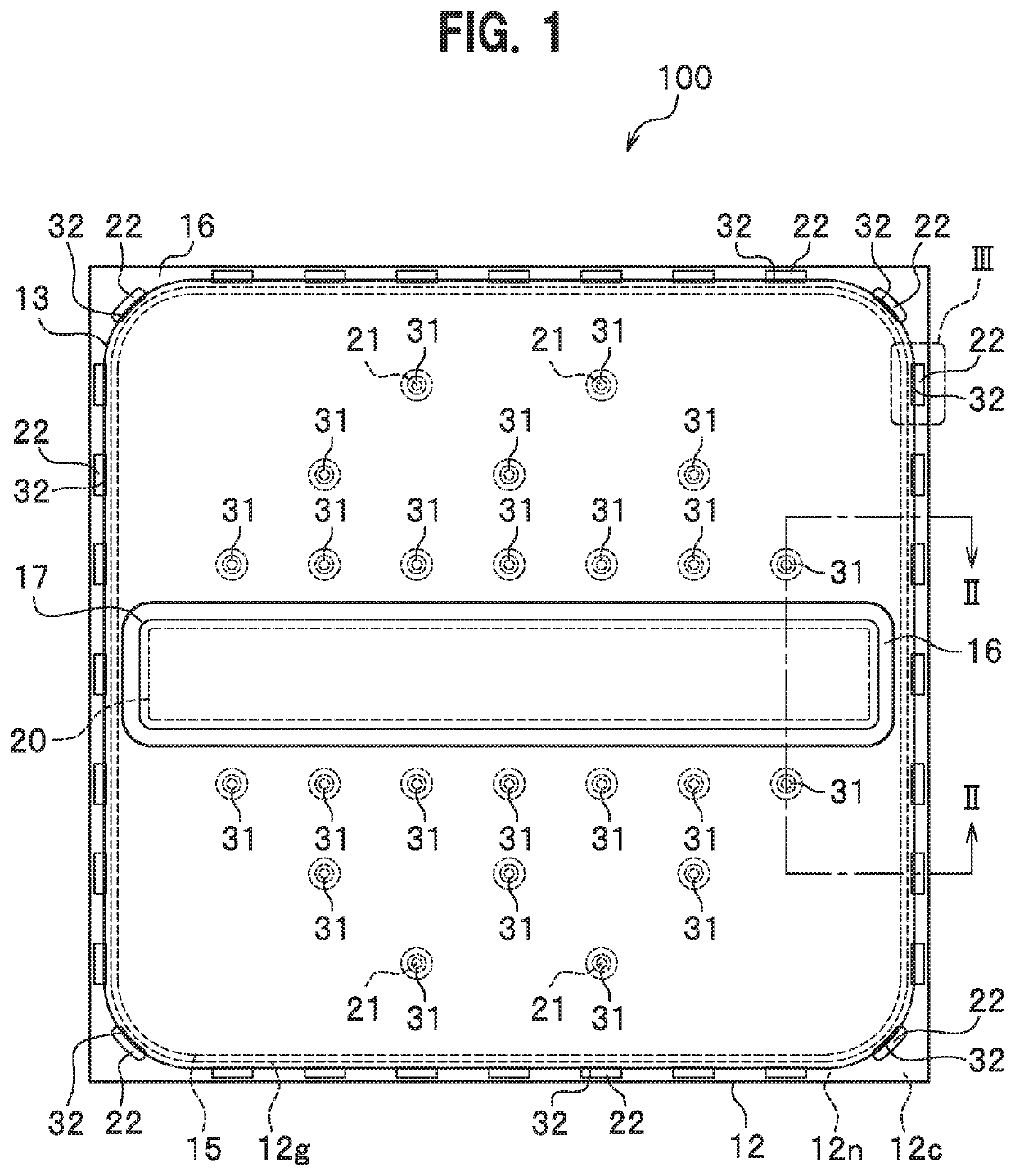
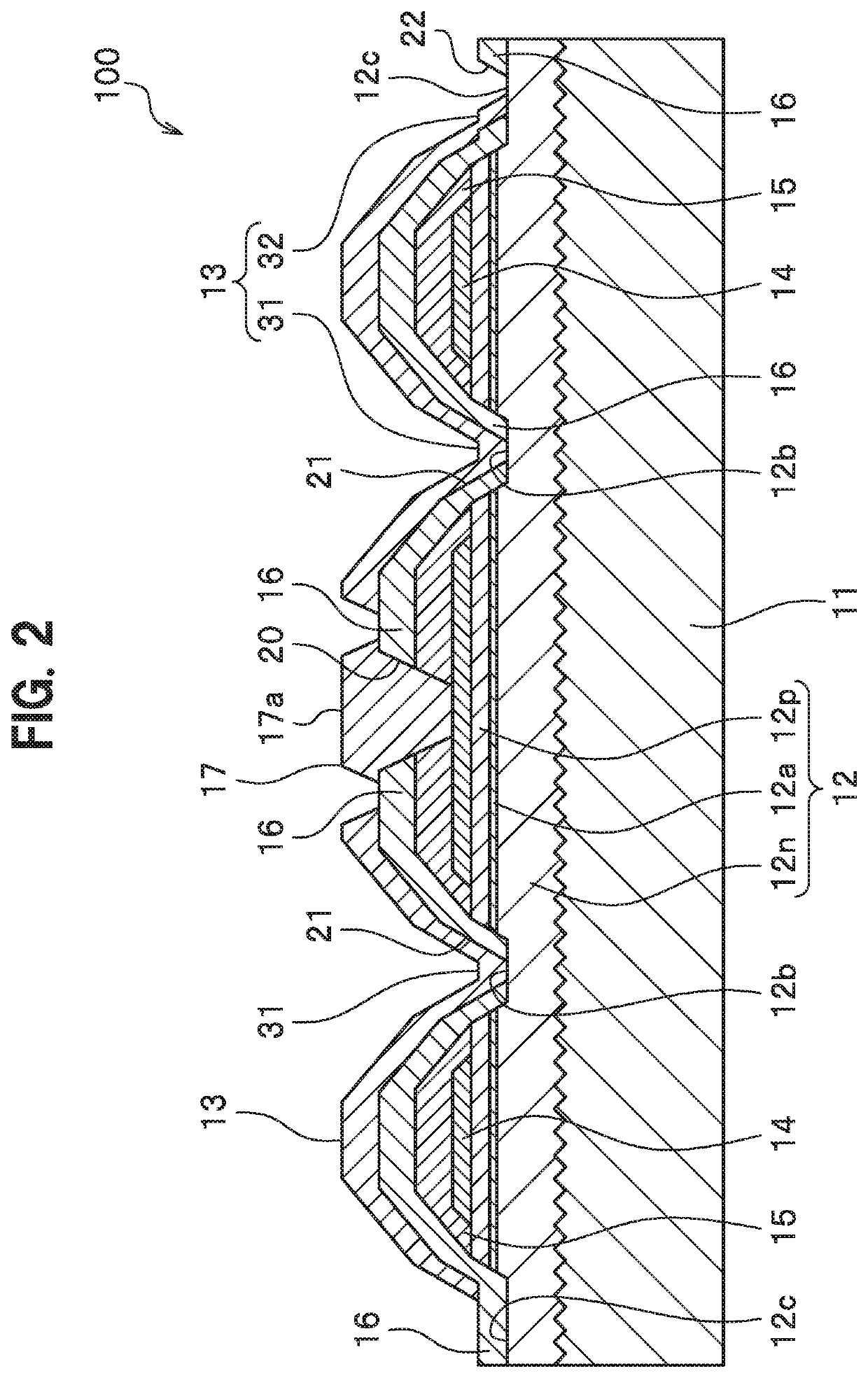
[0030]The semiconductor light emitting element 100 according to the present embodiment has a LED (light emitting diode) structure. As shown in FIG. 2, an upper surface of the semiconductor light emitting element 100 is a mounting surface to be electrically connected to the outside. Further, a lower surface of the semiconductor light emitting element 100 is a light extraction surface. The semiconductor light emitting element 100 is prepared in a state of a wafer, which will be described below in detail.

[0031]Structures of pa...

second embodiment

[0103]As shown in FIG. 15, a semiconductor light emitting element 100B according to a second embodiment is different from the semiconductor light emitting element 100 according to the first embodiment in shape of the semiconductor layered body 12. Hereinafter, the same configurations as in the semiconductor light emitting element 100 shown in FIG. 1 are provided with the same reference numerals, and descriptions thereof are omitted.

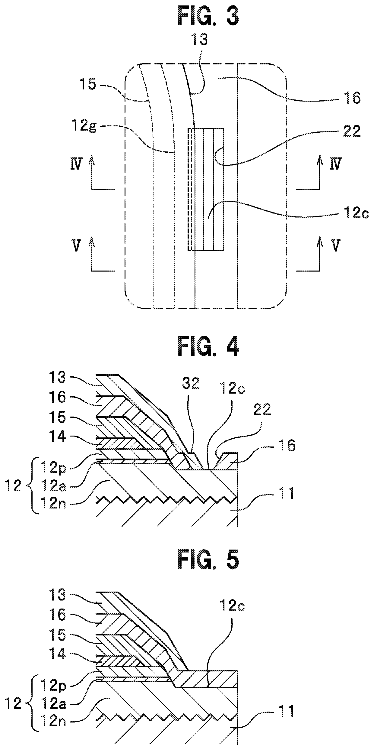
[0104]The semiconductor light emitting element 100B is different from the semiconductor light emitting element 100 shown in FIG. 1 in that, in a top view, an outer peripheral region 12c of an n-side semiconductor layer 12n has extending regions 90 extending toward an inner region 12g, an insulating film 16 defines second n-side openings 22 each formed in a respective one of the extending regions 90, and an n-electrode 13 is formed to cover the second n-side openings 22 each defined in a respective one of the extending regions 90.

[0105]In the present embod...


PUM

PropertyMeasurementUnit
semiconductoraaaaaaaaaa
areaaaaaaaaaaa
areasaaaaaaaaaa

Abstract

A semiconductor light emitting element includes a semiconductor layered body including an n-side semiconductor layer and a p-side semiconductor layer disposed above the n-side semiconductor layer, an insulating film defining a plurality of first n-side openings on the n-side semiconductor layer in an inner region and a plurality of second n-side openings on an outer peripheral region of the n-side semiconductor layer, an n-electrode disposed extending over the insulating film and the outer peripheral region of the n-side semiconductor layer and including: a plurality of first n-contact portions, each electrically connected with the n-side semiconductor layer through a respective one of the first n-side openings, and a plurality of second n-contact portions, each electrically connected with the n-side semiconductor layer through a respective one of the second n-side openings, at at least four corners of the outer peripheral region of the n-side semiconductor layer.

Description

CROSS-REFERENCE TO RELATED APPLICATIONS[0001]This application claims priority to Japanese Patent Application No. 2018-143113, filed on Jul. 31, 2018, the entire contents of which are incorporated herein by reference.BACKGROUND1. Technical Field[0002]The present disclosure relates to a semiconductor light emitting element.2. Description of Related Art[0003]Flip-chip-mounted semiconductor light emitting elements are known (see, for example, JP 2017-135348 A). The semiconductor light emitting element described in JP 2017-135348 A includes, as electrodes for external connection, a p-pad electrode electrically connected to a p-side semiconductor layer of a semiconductor layered body and disposed at the central region of the semiconductor light emitting element in a top view, and n-electrodes disposed on both sides of the p-pad electrode. In the semiconductor light emitting element, the n-pad electrode includes a plurality of n-contact portions dispersedly disposed in regions excluding th...

Claims


Application Information

Patent Timeline
Patent Type & Authority Patents(United States)
IPC IPC(8): H01L33/38H01L33/62H01L33/36
CPCH01L33/62H01L33/36H01L33/38H01L33/387H01L33/382H01L33/44
Inventor MIKI, YASUHIROTAKENAGA, KOICHI
Owner NICHIA CORP
Why Eureka
Try Eureka