Array substrate and OLED display device

a display device and substrate technology, applied in the field of display technologies, can solve the problems of affecting the display effect of the screen, the process of the screen may be risky, and the coupling capacitance exists, so as to reduce the coupling effect between the two layers of trace, reduce the ir drop withou, and increase the capacitance

Active Publication Date: 2021-02-09
WUHAN CHINA STAR OPTOELECTRONICS SEMICON DISPLAY TECH CO LTD
View PDF8 Cites 1 Cited by
  • Summary
  • Abstract
  • Description
  • Claims
  • Application Information

AI Technical Summary

Benefits of technology

[0008]The object of the present application is to provide an array substrate and an OLED display device, which can reduce IR drop, improve the display uniformity of the display device, reduce the coupling storage capacitance between the traces, and a storage capacitor with larger capacitance can be formed.
[0012]The beneficial effect: the trace system of the array substrate is designed in a structure with three layers of metal, which facilitates to obtain a circuit designed with a larger pixel per inch (PPI). By providing one layer of inorganic insulation film and one layer of organic insulation film between the two layers of metal, the coupling effect between the two layers of trace can be reduced. By exposing all or part of the organic insulation film in a region, which will form the second electrode plate of the storage capacitor, a storage capacitor with larger capacitance can be formed. By forming the third metal layer as a mesh structure, it is possible to reduce the IR drop without increasing the mask and improve the display uniformity of the display device. In addition, the present application is arranged in a mirror symmetrical structure, and the number of power lines, reset signal lines, and via holes can be reduced by about half, thereby providing space for pixels to realize a display device with high PPI.

Problems solved by technology

IR-drop in the active area (AA) of the existing array substrate during displaying causes an issue of uneven display of the screen, and the process thereof may have a risk.
Furthermore, coupling capacitance exists between the data line and the power line in the existing array substrate, and a thickness of the dielectric layer between two gate layers is limited; thereby, a storage capacitor with larger capacitance cannot be formed.

Method used


Image

  • Array substrate and OLED display device
  • Array substrate and OLED display device

Examples


Embodiment Construction

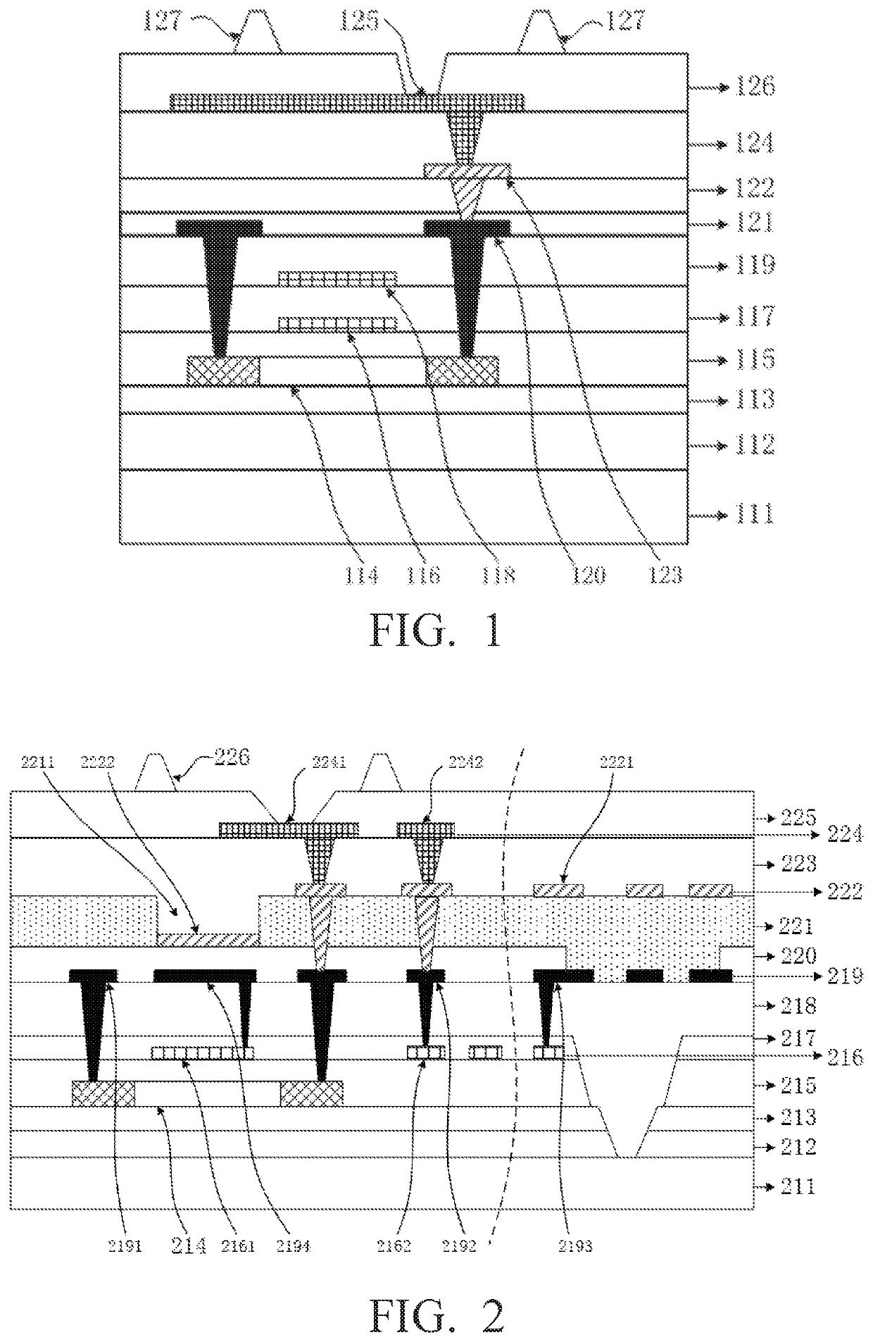
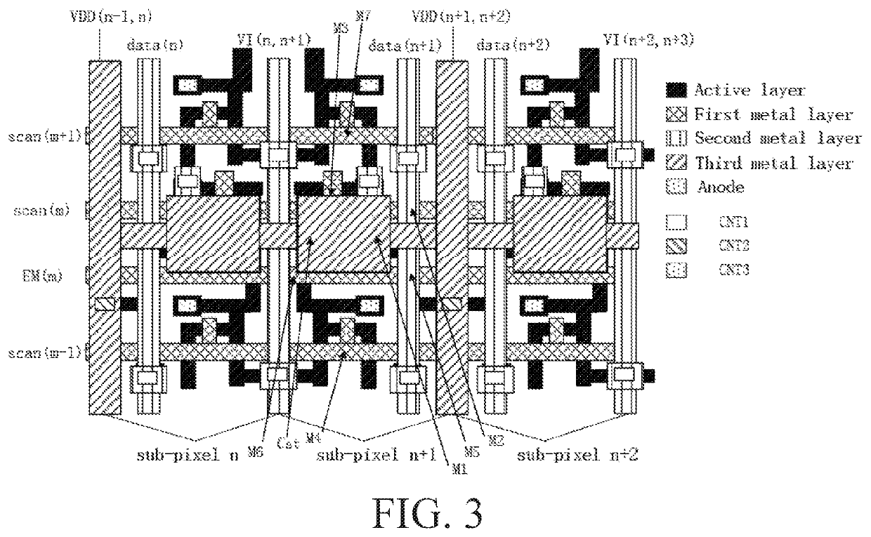
[0017]In the following detailed description of the preferred embodiments, reference is made to the accompanying drawings which form a part hereof, and in which is shown by way of illustrating specific embodiments in which the invention may be practiced. In this regard, directional terminology; such as “top”, “bottom”, “front”; “back”, “left”, “right”, “inside”, “outside”, “side”, etc., is used with reference to the orientation of the figure(s) being described. As such, the directional terminology is used for purposes of illustration and is in no way limiting. Throughout this specification and in the drawings, like parts will be referred to by the same reference numerals.

[0018]An array substrate of the present application includes a plurality of sub-pixels, each of the sub-pixels includes a drive thin film transistor (Driver TFT) and a storage capacitor. The array substrate further includes a first metal layer (GE1), a second metal layer (SD1), and a third metal layer (SD2). The firs...


PUM

PropertyMeasurementUnit
electric fieldaaaaaaaaaa
luminous efficiencyaaaaaaaaaa
luminanceaaaaaaaaaa

Abstract

An array substrate and an OLED display device are provided. A trace system of the array substrate is designed in a structure with three layers of metal. By providing one layer of inorganic insulation film and one layer of organic insulation film between two layers of metal, a coupling effect between two layers of trace can be reduced. By exposing all or part of an organic insulation film in a region, which will form a second electrode plate of a storage capacitor, a storage capacitor with larger capacitance can be formed. By forming a third metal layer as a mesh structure, it is possible to reduce IR drop without increasing mask and improve display uniformity of the display device.

Description

FIELD OF INVENTION[0001]The present invention relates to the field of display technologies, and more particularly, to an array substrate and an OLED display device.BACKGROUND OF INVENTION[0002]In recent years, due to the development of organic light emitting diode (OLED) display technology, curved displays and flexible displays have quickly entered into the market, and technical updates in related fields are also changing rapidly. OLED refers to a diode that emits light by carrier injection and recombination under the electric field driven by an organic semiconductor material and a luminescent material. The OLED display device has wider application range due to its advantages of lightweight, self-illumination, wide viewing angles, low driving voltage, high luminous efficiency, low power consumption, and fast response time.[0003]OLED is a current-driven device that emits light when a current flows through it, and the luminance of the light is determined by the current flowing through...

Claims


Application Information

Patent Timeline
Patent Type & Authority Patents(United States)
IPC IPC(8): H01L29/08H01L27/32H01L27/12
CPCH01L27/3265H01L27/3258H01L27/3262H01L27/3276H01L27/1255H01L27/124H10K59/121H10K59/1216H10K59/124H10K59/131H10K59/1213
Inventor XU, PINQUANWANG, WEI
Owner WUHAN CHINA STAR OPTOELECTRONICS SEMICON DISPLAY TECH CO LTD
Why Eureka
Try Eureka