Nitride semiconductor light-emitting device

a technology of nitride and semiconductor, which is applied in the direction of semiconductor devices, semiconductor lasers, laser details, etc., can solve the problems of reducing the luminous efficiency of the active layer and the crystal quality of the nitride semiconductor layer, and achieves the suppression of the generation of planar defects in the active layer and high luminous efficiency

Active Publication Date: 2021-02-16
USHIO DENKI KK
View PDF3 Cites 0 Cited by
  • Summary
  • Abstract
  • Description
  • Claims
  • Application Information

AI Technical Summary

Benefits of technology

[0026]According to the present invention, generation of planar defects in the active layer may be suppressed, so that a nitride semiconductor light-emitting device having high luminous efficiency is realized.

Problems solved by technology

However, a problem is known that, when growing the nitride semiconductor layer having increased In composition, a crystal quality of the nitride semiconductor layer is deteriorated and luminous efficiency in the active layer is lowered.

Method used


Image

  • Nitride semiconductor light-emitting device
  • Nitride semiconductor light-emitting device
  • Nitride semiconductor light-emitting device

Examples


Embodiment Construction

0]A nitride semiconductor light-emitting device of the present invention is described with reference to the drawings. Note that, in each drawing, a dimensional ratio in the drawing does not necessarily coincide with an actual dimensional ratio.

Structure

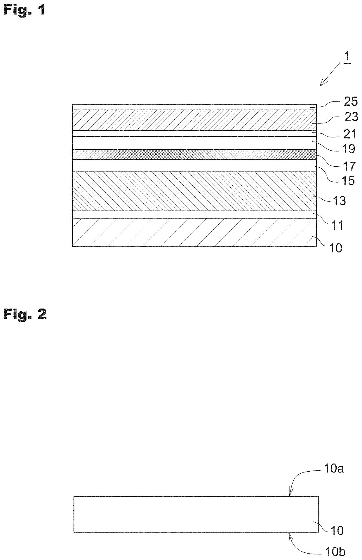
[0041]FIG. 1 is a cross-sectional view schematically illustrating a structure of one embodiment of a nitride semiconductor light-emitting device. A nitride semiconductor light-emitting device 1 is provided with a nitride semiconductor substrate 10, a first semiconductor layer 13, a second semiconductor layer 15, an active layer 17, and a third semiconductor layer 23.

[0042]Note that, in the example illustrated in FIG. 1, the nitride semiconductor device 1 is further provided with a fourth semiconductor layer 11, a fifth semiconductor layer 19, a sixth semiconductor layer 21, and a seventh semiconductor layer 25.

Nitride Semiconductor Substrate 10

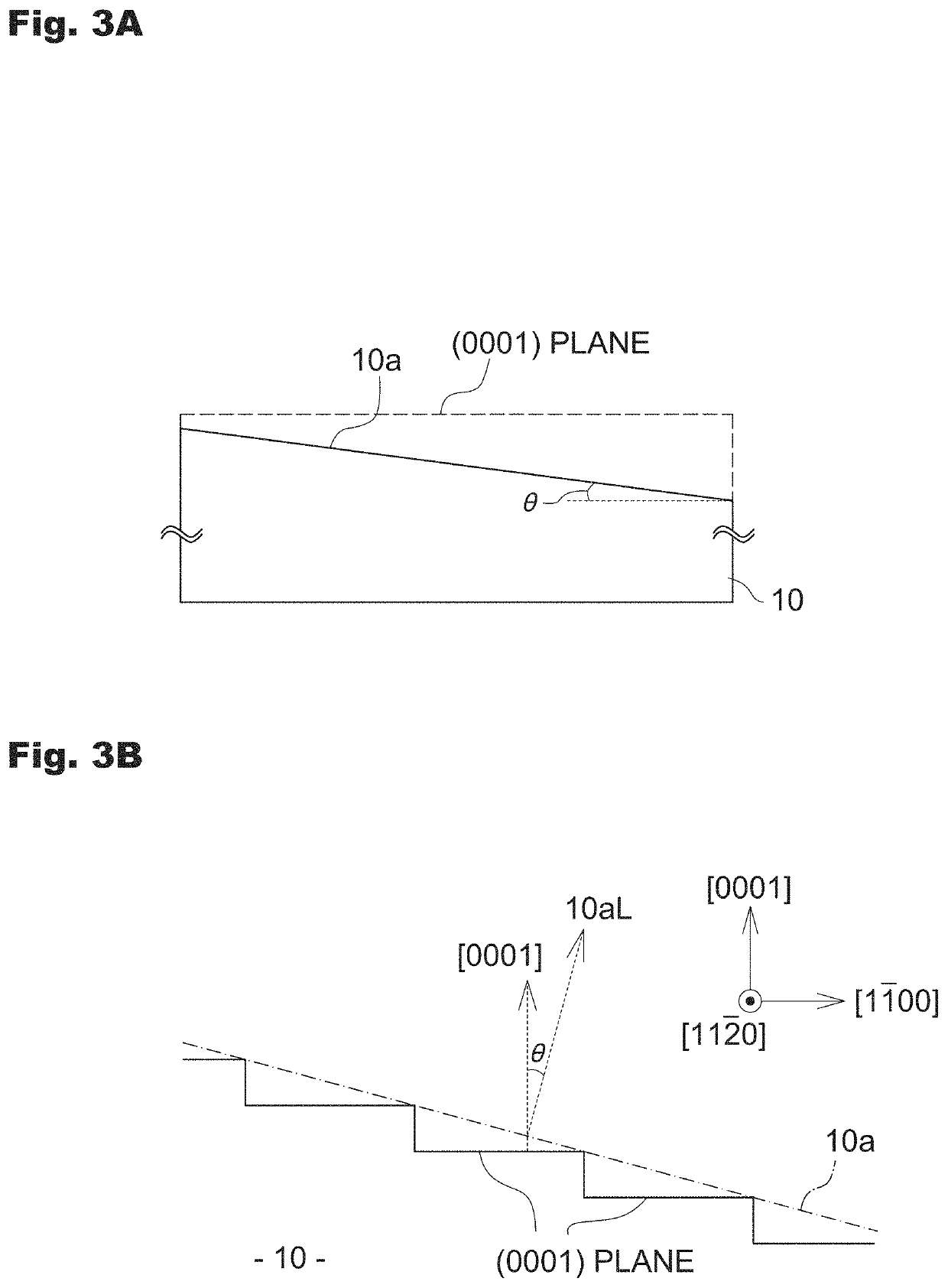
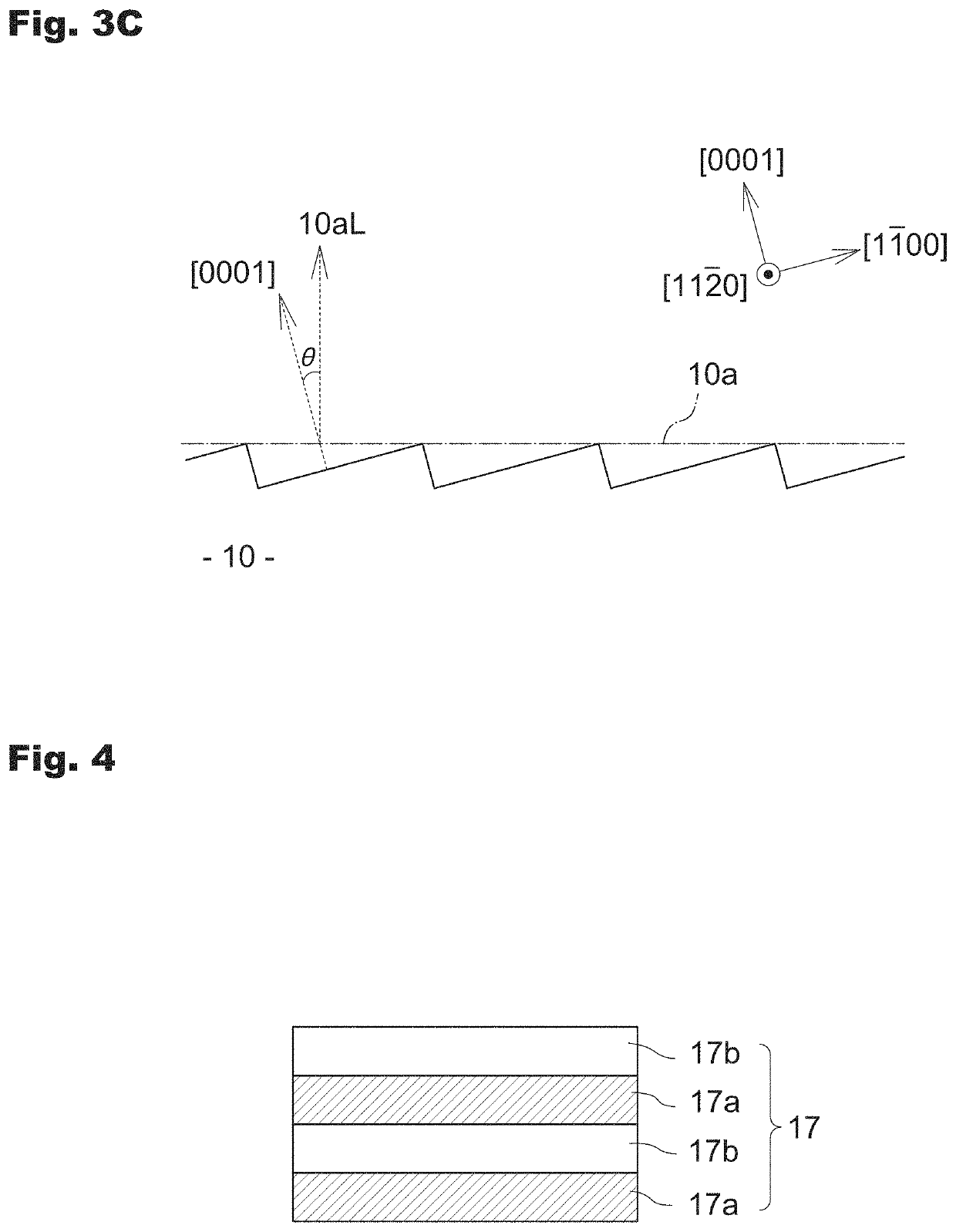
[0043]The nitride semiconductor substrate 10 is formed of GaN, AlGaN, or AlInGaN, and prefer...


PUM

PropertyMeasurementUnit
off angleaaaaaaaaaa
thicknessaaaaaaaaaa
emission wavelengthaaaaaaaaaa

Abstract

A nitride semiconductor light-emitting device having high luminous efficiency is provided. A nitride semiconductor light-emitting device is provided with a nitride semiconductor substrate including a main surface having an off angle of 0.4° or larger with respect to a (0001) plane, a first semiconductor layer formed of an n-type or p-type nitride semiconductor formed on the main surface, a second semiconductor layer formed of a nitride semiconductor having In composition of 2% or higher formed on the first semiconductor layer, an active layer formed on the second semiconductor layer including a well layer formed of a nitride semiconductor having In composition higher than that of the second semiconductor layer and a barrier layer formed of a nitride semiconductor stacked therein, and a third semiconductor layer formed on the active layer having a conductivity type different from that of the first semiconductor layer.

Description

BACKGROUND OF THE INVENTIONField of the Invention[0001]The present invention relates to a nitride semiconductor light-emitting device, and especially relates to a nitride semiconductor light-emitting device provided with a nitride semiconductor substrate.Description of the Related Art[0002]A nitride semiconductor light-emitting device is a device including a nitride semiconductor and is known as a light-emitting device capable of covering a wavelength range from an ultraviolet region to a visible light region in principle. Among the nitride semiconductors, GaN has a bandgap of 3.4 eV and InN has a bandgap of 0.8 eV. Therefore, by forming an active layer of InGaN which is a mixed crystal of InN and GaN and by changing In composition thereof, it is possible to realize a light-emitting device with an emission wavelength from 365 nm to 1550 nm in principle. That is, in order to shift the emission wavelength from 365 nm to a longer wavelength side, it is necessary to increase the In comp...

Claims


Application Information

Patent Timeline
Patent Type & Authority Patents(United States)
IPC IPC(8): H01S5/343H01S5/02H01S5/042
CPCH01S5/34333H01S5/0206H01S5/34346H01S5/0425H01S2304/04H01L21/02389H01L21/02433H01L21/02458H01L21/02505H01L21/0254H01L33/16H01L33/32H01S5/2201H01S5/2238H01S5/3213H01S5/3407H01S5/04254H01S5/04257H01S5/32025
Inventor MIYOSHI, KOHEINANIWAE, KOICHI
Owner USHIO DENKI KK
Why Eureka
Try Eureka