Optical module

a technology of optical modules and optical coupling, which is applied in the field of optical modules, can solve the problems of reducing the optical coupling efficiency of the semiconductor laser and the waveguide, adversely affecting the resonance state of the semiconductor laser, etc., and achieves the effect of reducing the return light beam and high optical coupling efficiency

Active Publication Date: 2021-03-23
NICHIA CORP
View PDF33 Cites 0 Cited by
  • Summary
  • Abstract
  • Description
  • Claims
  • Application Information

AI Technical Summary

Benefits of technology

[0006]The present disclosure has been made in view of the above problem, and it is an object of the present invention to provide an optical module that has high optical coupling efficiency between a semiconductor laser and a waveguide and is capable of reducing a return light beam from the waveguide to the semiconductor laser.
[0008]As described above, according to the present disclosure, it is possible to provide the optical module that has high optical coupling efficiency between the semiconductor laser and the waveguide and is capable of reducing a return light beam from the waveguide to the semiconductor laser.

Problems solved by technology

In such an optical module, a return light beam from the waveguide to the semiconductor laser may adversely affect a resonance state of the semiconductor laser.
However, when an emission surface of the semiconductor laser and the end surface of the substrate are arranged oblique to each other, a distance between a light-emitting point of the semiconductor laser and an incident surface of the waveguide becomes large because the light-emitting point is typically positioned approximately at a center in a width direction of the semiconductor laser, which leads to a decrease in optical coupling efficiency of the semiconductor laser and the waveguide.

Method used


Image

  • Optical module
  • Optical module
  • Optical module

Examples


Embodiment Construction

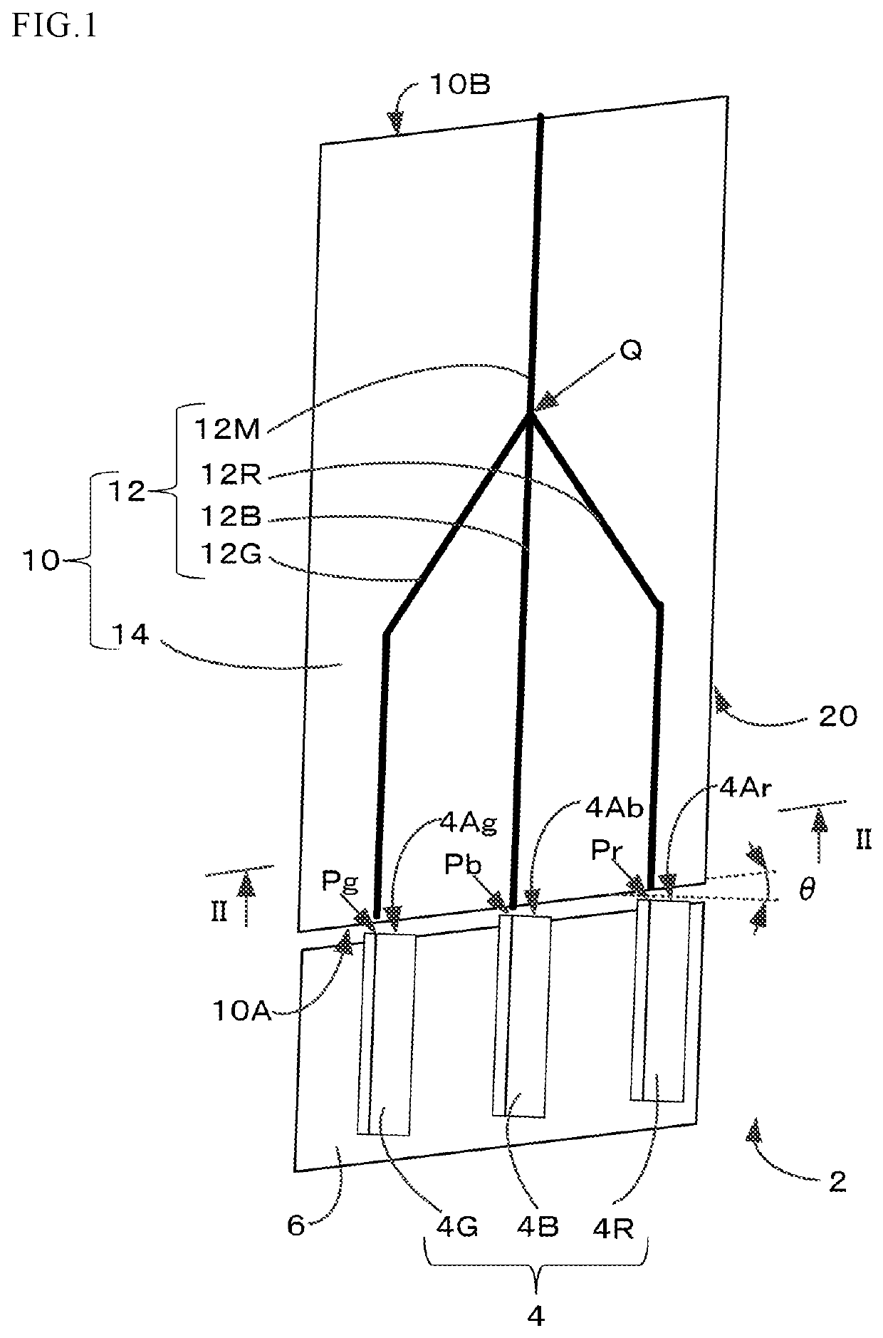
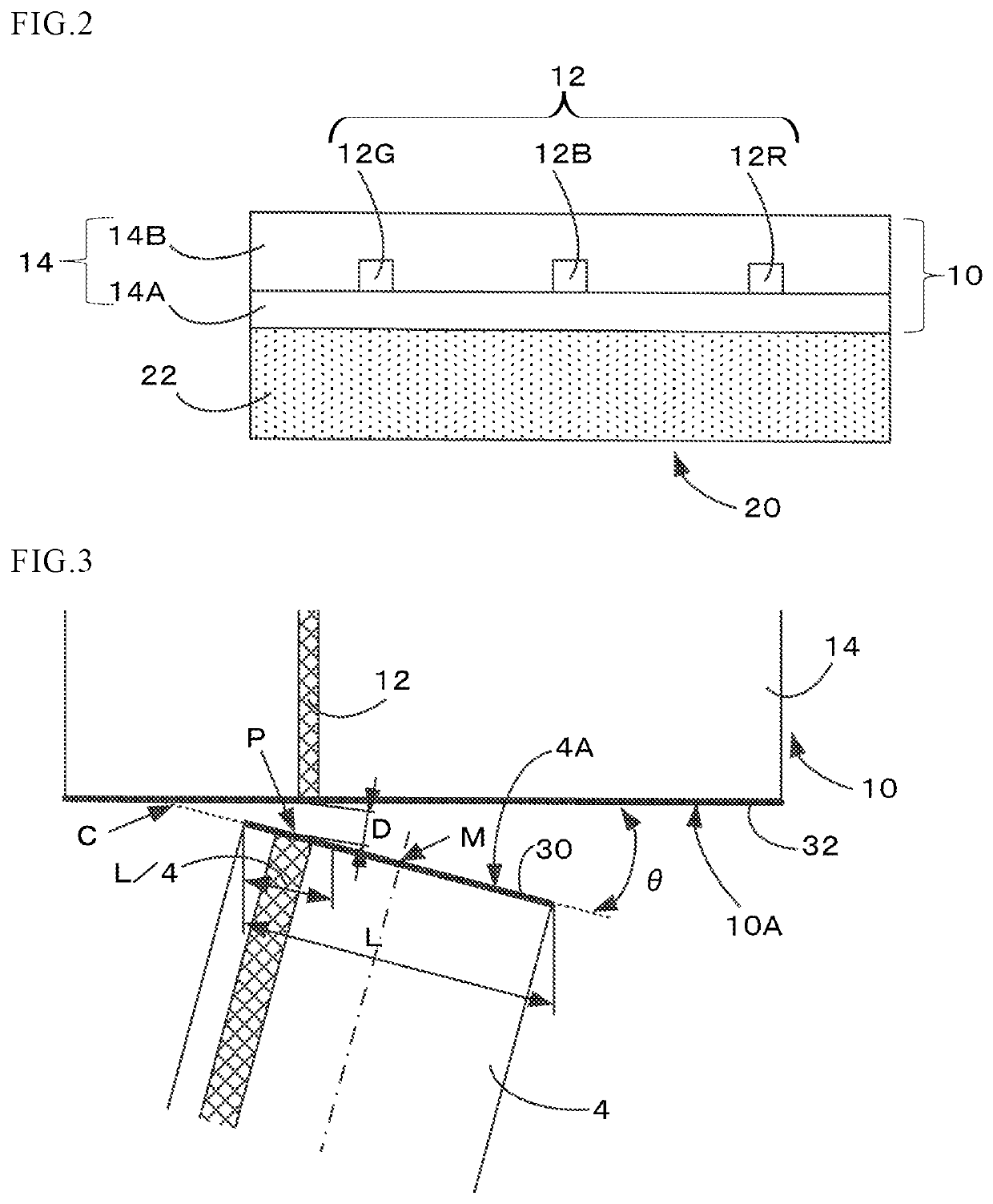
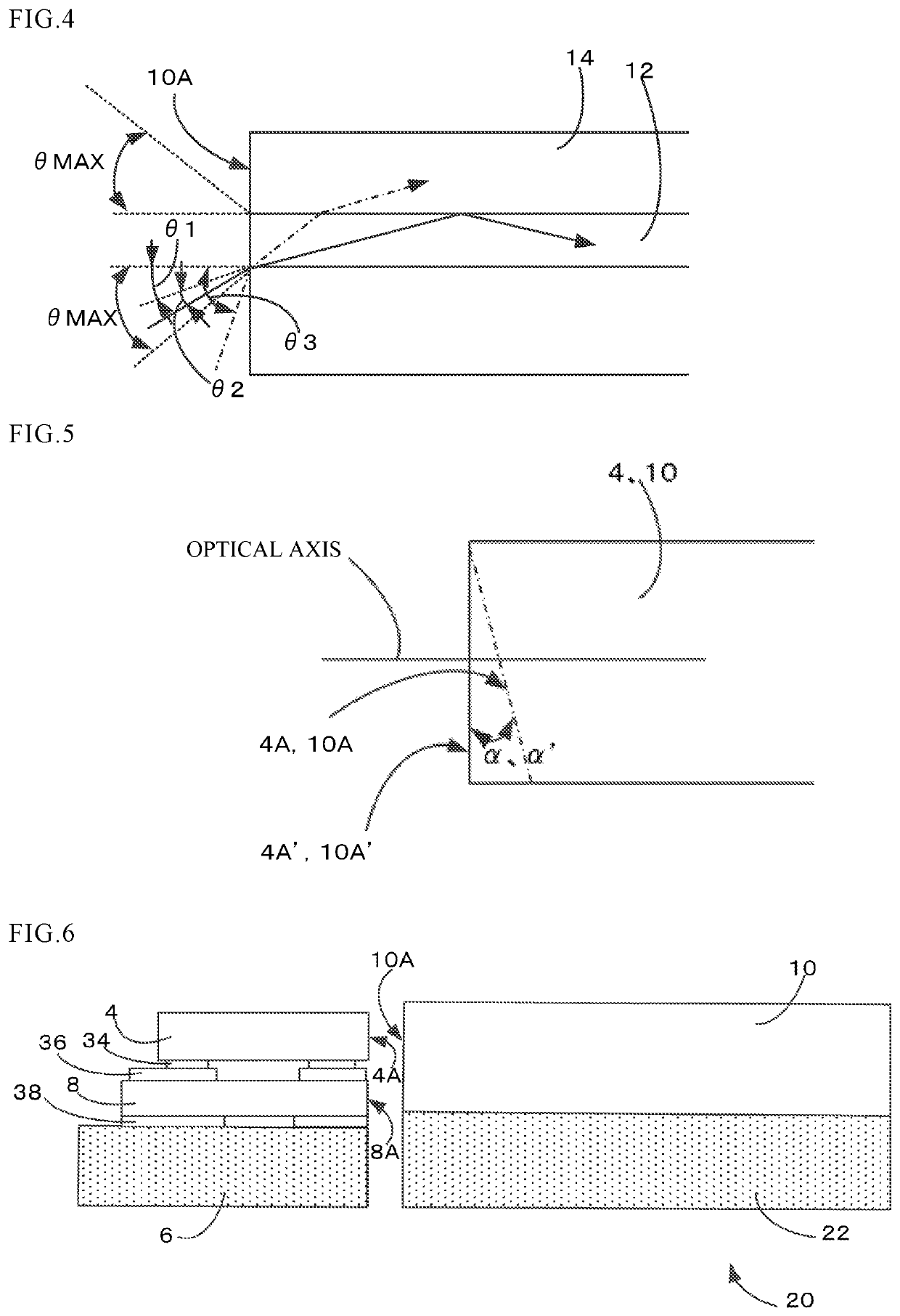
[0015]A description will hereinafter be given of an embodiment of the present invention with reference to the drawings. It is noted that an optical module described below is for embodying a technical idea of the present invention, and the present invention is not limited to the following unless otherwise specified.

[0016]In each of the drawings, components having the same function may be given the same reference numeral. Taking ease of explaining and understanding the gist into consideration, a description is given, for convenience of explanation, with a separate embodiment or example, but a partial substitution or combination of configurations shown in different embodiments and examples are possible. In the following embodiment and example, descriptions of matters common to previous descriptions are omitted, and only different points will be described. In particular, the similar actions and effects with the same configuration will not be consecutively mentioned for each embodiment o...


PUM

PropertyMeasurementUnit
lengthaaaaaaaaaa
divergence angleaaaaaaaaaa
acceptance angleaaaaaaaaaa

Abstract

There is provided an optical module comprising a semiconductor laser element; and a planar lightwave circuit (PLC) in which a waveguide is formed on a substrate. A position of a light-emitting point of the semiconductor laser element is approximately aligned with a position of a core of the waveguide. In a plan view, a first line segment representing an emission surface of the semiconductor laser element and a second line segment corresponding to the first line segment and representing an incident surface of the waveguide are arranged oblique to each other, and the light-emitting point of the semiconductor laser element is disposed closer to an intersection point of an extension line of the first line segment and the second line segment or an extension line of the second line segment than a center of the first line segment.

Description

CROSS-REFERENCE TO RELATED APPLICATIONS[0001]This application claims priority to Japanese Patent Application No. 2018-052126 filed on Mar. 20, 2018. The entire disclosure of Japanese Patent Application No. 2018-052126 is hereby incorporated herein by reference.BACKGROUNDTechnical Field[0002]The present invention relates to an optical module including a semiconductor laser and a waveguide.Related Art[0003]An optical module including a semiconductor laser and a waveguide optically connected with the semiconductor laser is in use in various industrial fields. In such an optical module, a return light beam from the waveguide to the semiconductor laser may adversely affect a resonance state of the semiconductor laser. In order to cope with the problem, there is proposed an optical module in which an end surface of a substrate on which a waveguide is formed and an end surface of the waveguide are formed at different angles (for example, see JP 2001-330744 A).SUMMARY[0004]In the optical mo...

Claims


Application Information

Patent Timeline
Patent Type & Authority Patents(United States)
IPC IPC(8): H01S5/10H01S5/022G02B6/42H01S5/026G02F1/39H01L31/0232G02F1/35H01S5/0239
CPCH01S5/1032G02B6/42G02F1/3501G02F1/395H01L31/0232H01S5/022H01S5/026H01S5/1085G02F2001/3509G02B6/4207G02B6/4202H01S5/4093H01S5/4012H01S5/021G02F1/3509H01S5/02325H01S5/0239
Inventor MIYATA, TADAAKI
Owner NICHIA CORP
Why Eureka
Try Eureka