Optical semiconductor device

a technology of optical coupling and semiconductor, applied in semiconductor lasers, laser optical resonator construction, laser details, etc., can solve the problem of inability to achieve high coupling efficiency, and achieve the effect of high optical coupling efficiency and suppression of leakage curren

Active Publication Date: 2017-02-07
MITSUBISHI ELECTRIC CORP
View PDF11 Cites 0 Cited by
  • Summary
  • Abstract
  • Description
  • Claims
  • Application Information

AI Technical Summary

Benefits of technology

[0006]In view of the above-described problems, an object of the present invention is to provide an optical semiconductor device capable of making electrical separation between the semiconductor laser section and the optical waveguide section compatible with high optical coupling efficiency.
[0008]In the present invention, since the second Fe-doped semiconductor layer is provided on the p-type semiconductor layer side on the semiconductor laser section, it is possible to suppress a leakage current from the p-type semiconductor layer on the semiconductor laser section to the optical waveguide section. Even when the second Fe-doped semiconductor layer is provided, no reflection or scattering of light occurs when light from the semiconductor laser section is coupled with the optical waveguide section. Therefore, it is possible to make electrical separation between the semiconductor laser section and the optical waveguide section compatible with high optical coupling efficiency.

Problems solved by technology

However, when the separation groove that electrically separates the semiconductor laser section from the optical waveguide section is deepened, light may be reflected or scattered when light from the semiconductor laser section is coupled with the optical waveguide section, which results in a problem that high coupling efficiency cannot be achieved.

Method used


Image

  • Optical semiconductor device
  • Optical semiconductor device
  • Optical semiconductor device

Examples


first embodiment

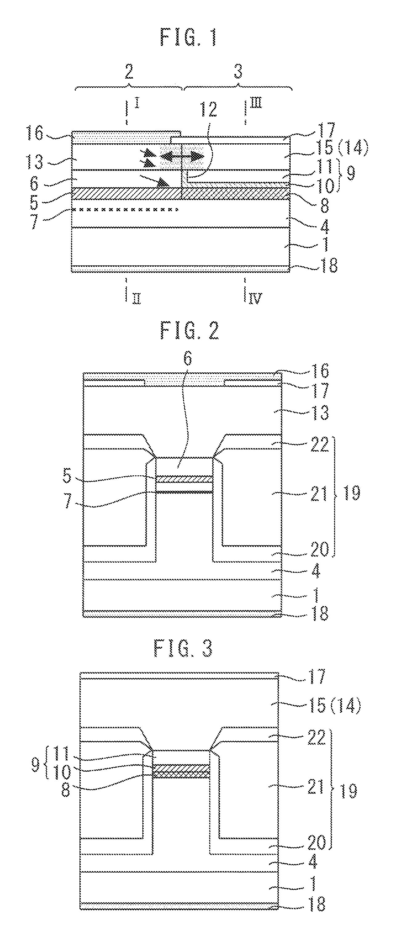
[0018]FIG. 1 is a cross-sectional view illustrating an optical semiconductor device according to a first embodiment of the present invention. FIG. 1 is a cross-sectional view of the optical semiconductor device cut in a resonator direction, that is, in a direction parallel to a traveling direction of laser light. This optical semiconductor device is an integrated optical semiconductor device in which a semiconductor laser section 2 and an optical waveguide section 3 are integrated on an n-type InP substrate 1.

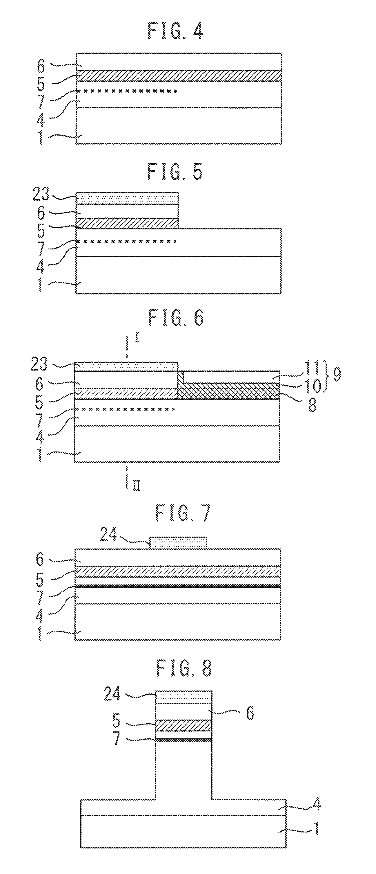
[0019]The semiconductor laser section 2 includes an n-type InP cladding layer 4, an active layer 5 and a p-type InP cladding layer 6 formed in that order on the n-type InP substrate 1. A diffraction grating 7 is formed in the n-type InP cladding layer 4 and the semiconductor laser section 2 is a distribution feedback type semiconductor laser. A carrier concentration of the n-type InP cladding layer 4 is 1×1018 cm−3. The active layer 5 is an AlGaInAs distortion quantum well acti...

second embodiment

[0040]FIG. 15 is a cross-sectional view illustrating an optical semiconductor device according to a second embodiment of the present invention. In the present embodiment, the leakage current suppression layer 14 further includes a low carrier concentration InP layer 27 having a lower carrier concentration than that of the p-type InP layer 13. The low carrier concentration InP layer 27 includes a side wall part 28 which is in contact with a side face of the p-type InP layer 13. The Fe-doped InP layer 15 is disposed on a side of the p-type InP layer 13 via the side wall part 28 of the low carrier concentration InP layer 27 and is not in contact with the p-type InP layer 13. The rest of the configuration is similar to that of the first embodiment.

[0041]Since the side wall part 28 of the low carrier concentration InP layer 27 exists between the p-type InP layer 13 on the semiconductor laser section 2 and the Fe-doped InP layer 15 on the optical waveguide section 3, a high-resistance pro...

third embodiment

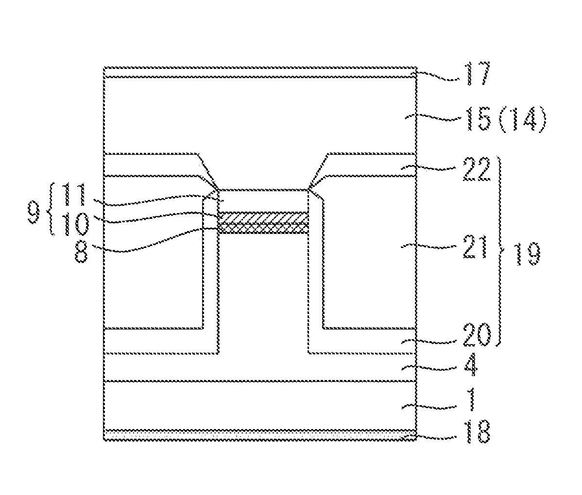
[0042]FIG. 16 is a cross-sectional view illustrating an optical semiconductor device according to a third embodiment of the present invention. FIG. 16 is a cross-sectional view of the optical waveguide section 3 cut along a direction perpendicular to the resonator direction. The p-type InP layer 13 is formed on the semiconductor laser section 2, the optical waveguide section 3 and the current constriction layer 19.

[0043]The current constriction layer 19 that embeds both sides of the semiconductor laser section 2 includes the p-type InP embedded layer 20, the Fe-doped InP embedded layer 21 and the n-type InP embedded layer 22 as in the case of FIG. 2 of the first embodiment. On the other hand, the current constriction layer 19 that embeds both sides of the optical waveguide layer 8 is the p-type InP embedded layer 20 and the Fe-doped InP embedded layer 21.

[0044]As the manufacturing method, after forming the embedded layer, n-type InP embedded layer 22 is removed from only the optical...


PUM


Abstract

An upper cladding layer includes a first low carrier concentration layer having a lower carrier concentration than the p-type cladding layer and a first Fe-doped semiconductor layer formed on the first low carrier concentration layer. The leakage current suppression layer includes a second Fe-doped semiconductor layer disposed on a side of the p-type semiconductor layer. The first low carrier concentration layer has a side wall part that is in contact with a side face of the p-type cladding layer. The first Fe-doped semiconductor layer is disposed on a side of the p-type cladding layer via the side wall part of the first low carrier concentration layer and is not in contact with the p-type cladding layer.

Description

BACKGROUND OF THE INVENTION[0001]Field of the Invention[0002]The present invention relates to an optical semiconductor device which integrates a semiconductor laser section and an optical waveguide section, and more particularly, to an optical semiconductor device capable of making electrical separation between a semiconductor laser section and an optical waveguide section compatible with high optical coupling efficiency.[0003]Background Art[0004]With a semiconductor laser, optical waveguide, optical modulator or the like integrated therein, optical semiconductor devices are becoming increasingly smaller in size and more sophisticated in performance. An integrated optical semiconductor device is known which integrates an optical active element typified by a semiconductor laser and an optical waveguide on a substrate. In such an integrated optical semiconductor device, a plurality of integrated components are generally electrically separated from each other. A p-type semiconductor la...

Claims


Application Information

Patent Timeline
Patent Type & Authority Patents(United States)
IPC IPC(8): H01S5/227H01S5/026H01S5/22H01S5/343H01S5/30H01S5/12H01S5/32
CPCH01S5/2275H01S5/026H01S5/12H01S5/2222H01S5/2224H01S5/3054H01S5/3211H01S5/34306H01S5/34366H01S2301/17H01S5/0261
Inventor SAKAINO, GO
Owner MITSUBISHI ELECTRIC CORP
Why Eureka
Try Eureka