Hybrid optoelectronic device

a technology of optoelectronic devices and hybrid devices, which is applied in the field of hybrid optoelectronic devices, can solve the problems of small productivity, high cost of group iii-v devices, and inability to achieve further miniatures in traditional silicon processes, etc., and achieves high optical coupling efficiency and large yield. the effect of productivity

Inactive Publication Date: 2013-08-01
NATIONAL TSING HUA UNIVERSITY
View PDF10 Cites 2 Cited by
  • Summary
  • Abstract
  • Description
  • Claims
  • Application Information

AI Technical Summary

Benefits of technology

[0010]Still another purpose of the invention is to provide an optoelectronic device manufactured with large yield and productivity, in which high optical coupling efficiency comes from the Group III-V active device to the Si passive device (optical access), making this device beneficial to the application to the photonic integrated circuit and suitable for future development of high-performance electronic and optoelectronic devices.

Problems solved by technology

However, with the physical limitations, the traditional silicon process cannot achieve the further miniature for the need of higher speed and lower cost.
However, Group III-V devices are generally more expensive than Si devices, because: (1) Group III-V compounds are rare elements; (2) the wafer size is small and therefore its productivity is small; and (3) the process is complicated, and therefore has low yield.
Therefore, the prior art cannot meet the need for the users in actual use.

Method used


Image

  • Hybrid optoelectronic device
  • Hybrid optoelectronic device
  • Hybrid optoelectronic device

Examples


Embodiment Construction

[0027]The aforementioned illustrations and following detailed descriptions are exemplary for the purpose of further explaining the scope of the present invention. Other objectives and advantages related to the present invention will be illustrated in the subsequent descriptions and appended tables.

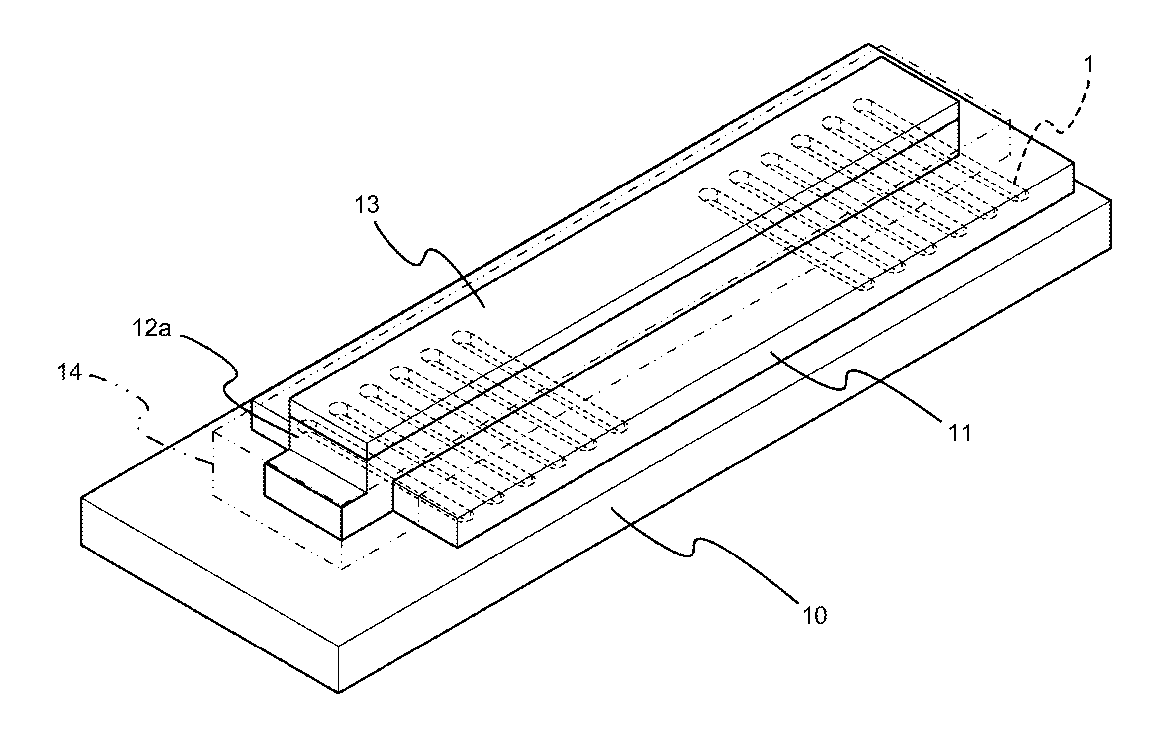
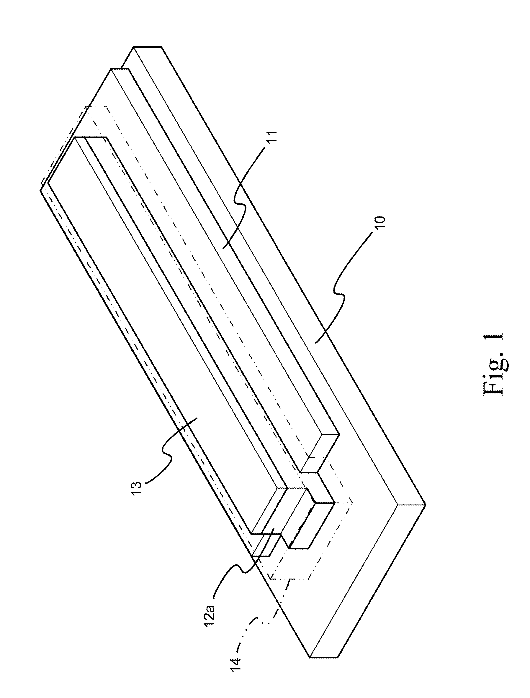
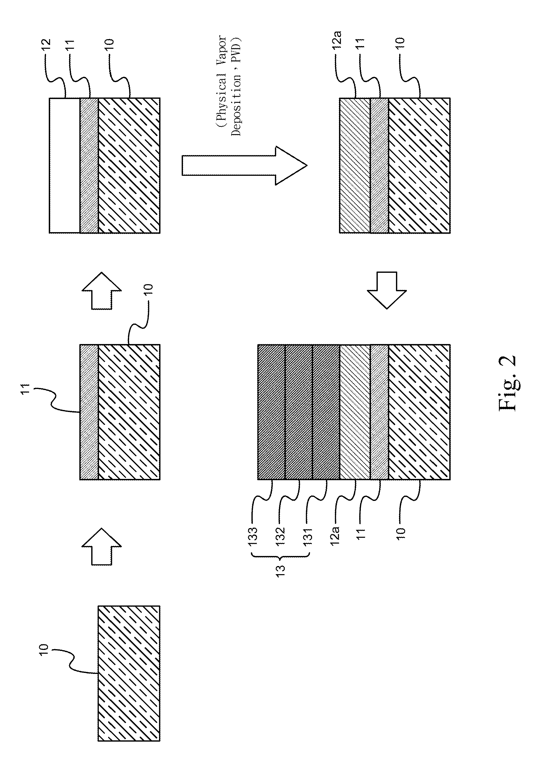
[0028]FIG. 1 is a schematic, perspective view of a hybrid optoelectronic (HOE) device according to the present invention. FIG. 2 is a schematic, cross-sectional view of a hybrid optoelectronic (HOE) device according to the present invention. FIG. 3 is a schematic view of epitaxial patterns of RE III-V structure of a hybrid optoelectronic (HOE) device according to the present invention. As shown, the hybrid optoelectronic (HOE) device according to the present invention includes a substrate 10, an insulating layer 11, a RMG structure 12a and an RE III-V structure 13.

[0029]The insulating layer 11 is formed on the substrate 10.

[0030]The RMG structure 12a is formed on the insulating layer 11. T...


PUM


Abstract

A hybrid optoelectronic device having Group III-V and Si composition on a low-cost substrate is disclosed. A photonic integrated circuit implemented by the hybrid optoelectronic device is much inexpensive and superior to those implemented by the conventional Group III-V optoelectronic device. In the hybrid optoelectronic device, a physical vapor deposition method is used to form a RMG structure with a smooth surface, and further produce a RE structure on the RMG structure. It relates a monolithic process. The wavelength and the material which attract interest can be adjusted. Thereby, the optoelectronic device can be manufactured with large yield and productivity. High optical coupling efficiency that can be offered comes from the Group III-V active device to the Si passive device (optical access). This would be beneficial to the application to the photonic integrated circuit and suitable for future development of high-performance electronic and optoelectronic devices.

Description

BACKGROUND OF THE INVENTION[0001]1. Field of the Invention[0002]The present invention relates to providing a hybrid optoelectronic device, and particularly to a device that has Group III-V and Si composition on a low-cost substrate such as Si or silicon-on-insulator (SOI) chip. More particularly, it relates to a device having a Re-epitaxy (RE) structure on a smooth surface of a rapid melt growth (RMG) structure by virtue of physical principle.[0003]2. Description of Related Art[0004]In the current semiconductor industry, the silicon process has been mature and widely used, and is the mainstream of the semiconductor material. However, with the physical limitations, the traditional silicon process cannot achieve the further miniature for the need of higher speed and lower cost. Group III-V semiconductor materials have been proposed in recent years due to the advantages of higher mobility and greater light absorption coefficient at optical communication wavelengths. However, Group III-...

Claims


Application Information

Patent Timeline
Patent Type & Authority Applications(United States)
IPC IPC(8): H01L31/12
CPCH01L31/125H01L21/02381H01L21/0245H01L21/02488H01L21/02502Y02E10/544H01L21/02667H01L31/1808H01L31/1852H01L31/1872H01L21/02546Y02P70/50
Inventor NA, YUN-CHUNG
Owner NATIONAL TSING HUA UNIVERSITY
Why Eureka
Try Eureka