
Packaging of a semiconductor device with dual sealing materials

a sealing material and semiconductor technology, applied in semiconductor devices, semiconductor/solid-state device details, electrical devices, etc., can solve the problems of sealing material peeled off the base plate, crack or the like may occur in the die-bonding portion, heat dissipation deterioration, etc., to reduce the thermal stress of the wiring member, suppress the peeled semiconductor element, and improve the reliability of the semiconductor device

Active Publication Date: 2021-05-11
MITSUBISHI ELECTRIC CORP
View PDF14 Cites 2 Cited by
  • Summary
  • Abstract
  • Description
  • Claims
  • Application Information

AI Technical Summary

Benefits of technology

The semiconductor device described in this patent is sealed with two different materials. The first material, a relatively hard material, prevents peeling of the semiconductor element, while the second material, a relatively soft material, protects the wiring member from dust and thermal stress. This helps to improve the reliability of the semiconductor device. Additionally, the first material ensures uniform sealing of the semiconductor element, while the second material ensures uniform sealing of the wiring member. This further improves the reliability of the semiconductor device.

Problems solved by technology

Therefore, there is the possibility that a crack or the like may occur in a die-bonding portion where the semiconductor element and the base plate are bonded together, due to thermal stress generated: in a die-bonding step of a manufacturing process; in temperature cycles in reliability evaluation; or the like, so that heat dissipation deteriorates.
However, there has been the possibility that the sealing material may be peeled off the base plate since a warp is caused in the base plate due to the difference between the expansion coefficients of the sealing material and the base plate.
There is the concern that a wire bonding portion may be damaged due to the peeling of the sealing material.

Method used


Image

  • Packaging of a semiconductor device with dual sealing materials
  • Packaging of a semiconductor device with dual sealing materials
  • Packaging of a semiconductor device with dual sealing materials

Examples


first embodiment

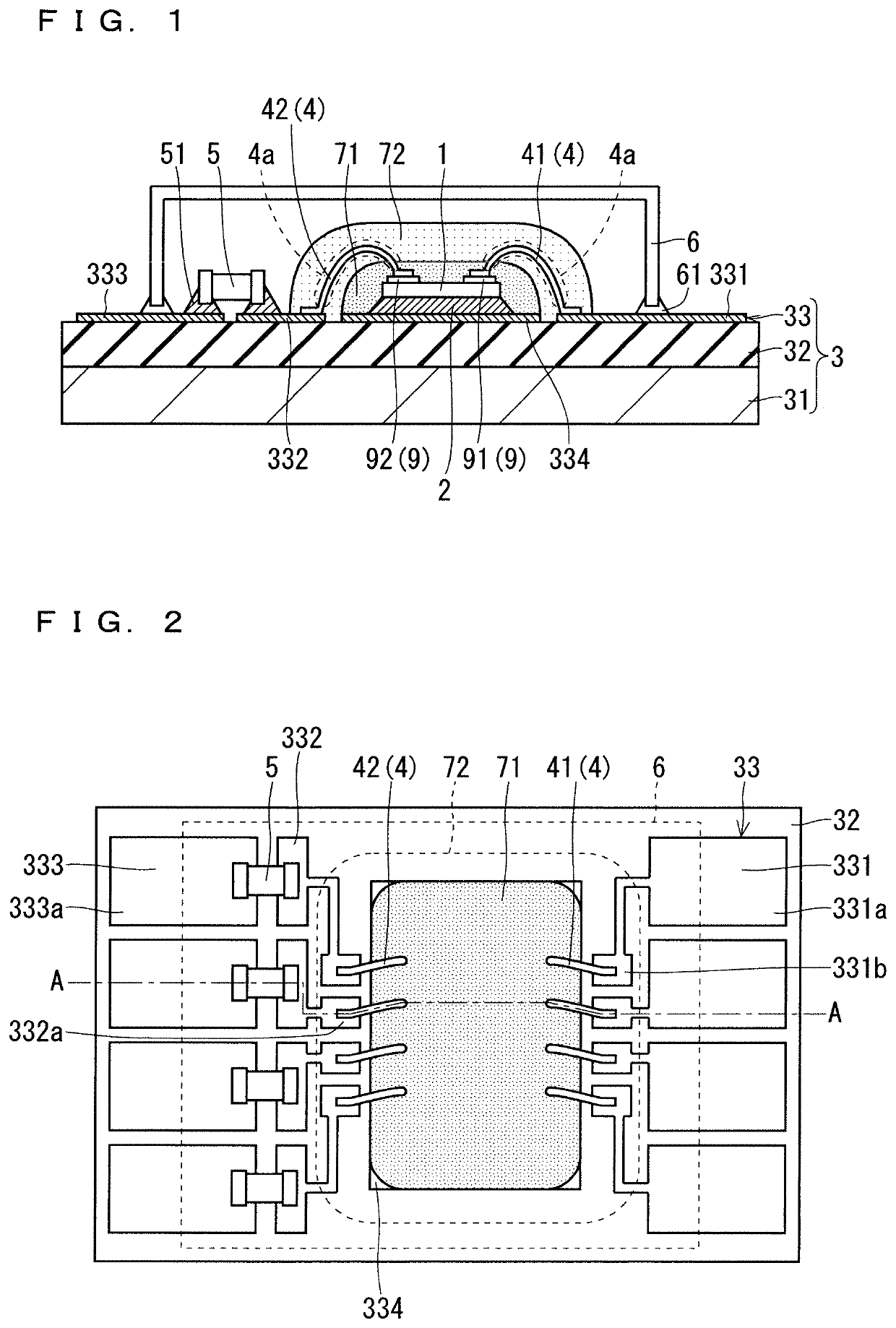
[0035]FIG. 1 is a cross sectional view of a semiconductor device according to a first embodiment. FIG. 2 is a plan view of the semiconductor device according to the first embodiment. The cross section of the semiconductor device illustrated in FIG. 1 is taken along line A-A of FIG. 2. In FIG. 2, a second sealing material 72 and a cap 6 are illustrated by virtual lines for easy understanding of the drawing.

[0036]The semiconductor device according to the first embodiment includes an insulating layer 32, a conductive layer 33, a heat dissipation plate 31, a semiconductor element 1, a plurality of wiring members 4, a first sealing material 71, and the second sealing material 72. A base substrate 3 is composed of the heat dissipation plate 31, the insulating layer 32, and the conductive layer 33. The insulating layer 32 is bonded to the upper surface of the heat dissipation plate 31. The conductive layer 33 is bonded to the upper surface of the insulating layer 32.

[0037]The plurality of ...

second embodiment

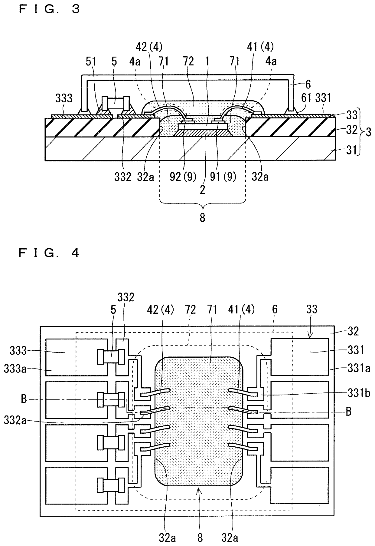
[0075]FIG. 3 is a cross sectional view of a semiconductor device according to a second embodiment. FIG. 4 is a plan view of the semiconductor device according to the second embodiment. The cross section of the semiconductor device illustrated in FIG. 3 is taken along line B-B of FIG. 4. In FIG. 4, a second sealing material 72 and a cap 6 are illustrated by virtual lines for easy understanding of the drawing.

[0076]In the second embodiment, an opening 8 is provided in almost the center of a base substrate 3. Since the length of a wiring member 4, one of the factors that reduce high frequency characteristics, can be shortened by providing the opening 8, a structure suitable for a high frequency semiconductor device can be achieved.

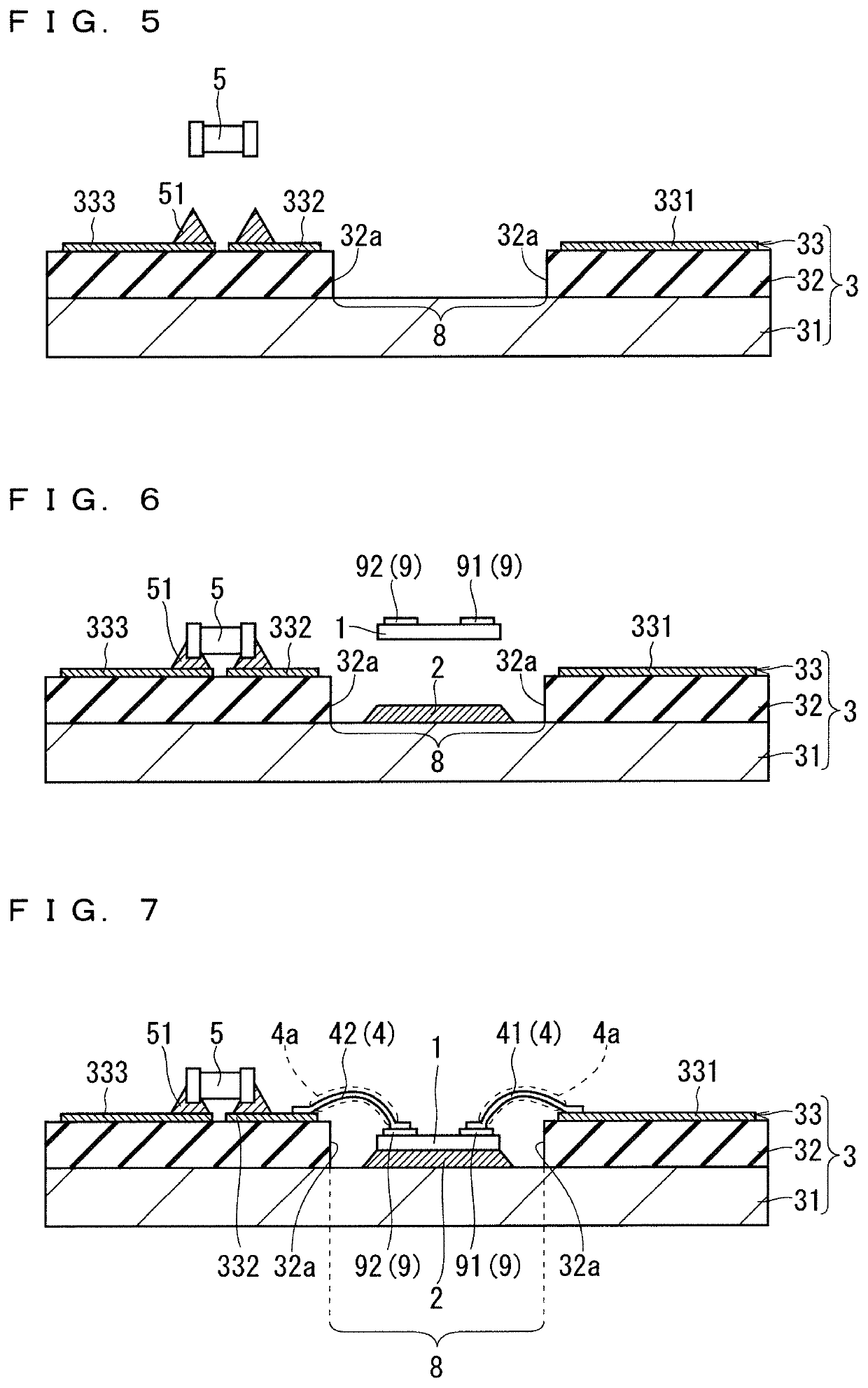
[0077]A heat dissipation plate 31 is not covered with an insulating layer 32 in the opening 8. The opening 8 is formed by cutting the insulating layer 32, for example, by machining. In the second embodiment, the opening 8 is provided in the base substrate 3, ...

third embodiment

[0103]FIG. 10 is a cross sectional view of a semiconductor device according to a third embodiment. FIG. 11 is a plan view of the semiconductor device according to the third embodiment. The cross section of the semiconductor device illustrated in FIG. 10 is taken along line C-C of FIG. 11. In FIG. 11, a second sealing material 72 and a cap 6 are illustrated by virtual lines for easy understanding of the drawing.

[0104]In the third embodiment, an opening 8 of a base substrate 3 is also sealed with a first sealing material 71 like the second embodiment. In the third embodiment, the opening 8 is further filled with the first sealing material 71 to a height higher than or equal to the height of one main surface (i.e., the upper surface) of an insulating layer 32, as illustrated in FIG. 10. The first sealing material 71 is arranged such that it may be in contact with the side surface of a conductive layer 33 but it is not in contact with the upper surface of the conductive layer 33.

[0105]F...


PUM

PropertyMeasurementUnit
diameteraaaaaaaaaa
temperatureaaaaaaaaaa

Abstract

The present invention provides a semiconductor device including an insulating layer, a conductive layer bonded to one main surface of the insulating layer, a semiconductor element arranged such that the upper surface of the semiconductor element faces a direction same as the one main surface of the insulating layer, an upper electrode provided on the upper surface of the semiconductor element, a wiring member that has one end electrically bonded to the upper electrode of the semiconductor element and has another end electrically bonded to the conductive layer, and has a hollow portion, a first sealing material, and a second sealing material, in which the first sealing material seals at least part of the semiconductor element so as to be in contact with the semiconductor element, and the second sealing material seals the wiring member so as to be in contact with the wiring member.

Description

TECHNICAL FIELD[0001]The present invention relates to a semiconductor device, and for example, to a semiconductor device that handles high frequency signals.BACKGROUND ART[0002]In recent years, speeding up communication of mobile communication devices such as mobile phones and smart phones has become a trend with the spread of the Internet. Also, demand for safety is increasing, such as necessity of transmission and reception of images through disaster prevention radio communication. Along with this, increasing the reliability of high frequency communication packages, which are key devices, is urgently needed.[0003]High frequency packages are semiconductor devices that input and output signals of frequencies higher than several tens of MHz, while amplifying and matching the signals. With the demand for speeding up communication, high output of semiconductor devices is required. In a semiconductor device with a high output, a package structure with high heat dissipation is required. ...

Claims


Application Information

Patent Timeline
Patent Type & Authority Patents(United States)
IPC IPC(8): H01L23/31H01L23/08H01L23/29H01L23/433H01L23/00
CPCH01L23/3142H01L23/08H01L23/29H01L23/4334H01L24/48H01L23/12H01L23/50H01L23/13H01L23/49838H01L23/3135H01L23/3121H01L23/04H01L2224/8592H01L2224/73265H01L2224/48472H01L2224/49175H01L2924/19105H01L2224/48227H01L2224/32227H01L2224/05624H01L2224/291H01L2224/2929H01L2224/8384H01L2224/29294H01L2224/32245H01L2924/15153H01L2224/8392H01L23/66H01L2924/161H01L2924/1424H01L2924/142H01L24/85H01L2224/29339H01L24/83H01L24/92H01L2224/92247H01L2924/10161H01L24/45H01L24/05H01L2224/04042H01L24/29H01L24/32H01L2224/49113H01L24/49H01L2224/4911H01L2924/00015H01L2224/48091H01L2223/6655H01L25/16H01L2224/29147H01L2224/29344H01L2224/85424H01L2224/29116H01L2224/85447H01L2224/85439H01L2224/29117H01L2224/29111H01L2224/29144H01L2224/29138H01L2224/45124H01L2224/29347H01L2224/29355H01L2224/29363H01L2224/85444H01L2224/29364H01L2924/15192H01L2924/351H01L2924/3511H01L2924/00014H01L2924/014H01L2924/0665H01L2224/8512H01L2924/01014H01L2924/01079H01L2924/01006H01L2924/01047H01L2924/01029H01L2924/0105H01L2924/01032H01L2924/013
Inventor SAKAMOTO, SOICHIFUJINO, JUNJIKAWASHIMA, HIROSHIMAEDA, TAKETOSHI
Owner MITSUBISHI ELECTRIC CORP
Learn More