Supercharge Your Innovation With Domain-Expert AI Agents!

Patterned epitaxial substrate and semiconductor structure

a technology of epitaxial substrate and semiconductor structure, applied in the direction of semiconductor devices, electrical equipment, basic electric elements, etc., can solve the problems of reducing and achieve the effect of preventing the warpage of the edge and improving the yield of subsequent manufacturing processes

Active Publication Date: 2021-07-13
PLAYNITRIDE DISPLAY CO LTD
View PDF3 Cites 2 Cited by
  • Summary
  • Abstract
  • Description
  • Claims
  • Application Information

AI Technical Summary

Benefits of technology

The patent describes a patterned epitaxial substrate that can prevent edge warping during heating processes and improve subsequent manufacturing yields. The substrate features patterns that are integrally formed, with different sizes in different zones. This results in better photoelectric properties and reliability in semiconductor structures utilizing the patterned substrate.

Problems solved by technology

The thermal temperature difference or the difference in the thermal expansion coefficient in a heating process and a lattice mismatch lead to uneven distribution of stresses, stress unevenness, thus causing warpage of the edge of the epitaxial substrate and resulting in a decrease in yield of subsequent manufacturing processes.

Method used


Image

  • Patterned epitaxial substrate and semiconductor structure
  • Patterned epitaxial substrate and semiconductor structure
  • Patterned epitaxial substrate and semiconductor structure

Examples


Embodiment Construction

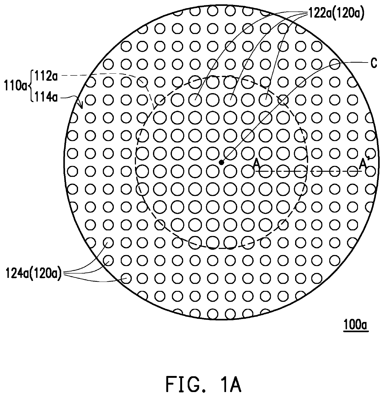
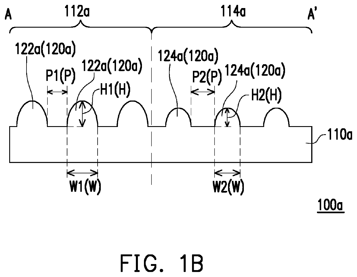
[0042]FIG. 1A is a schematic top view of a patterned epitaxial substrate according to an embodiment of the disclosure. FIG. 1B is a schematic cross-sectional view of the patterned epitaxial substrate depicted in FIG. 1A along a line segment A-A′. With reference to FIG. 1A, a patterned epitaxial substrate 100a provided in the embodiment includes a substrate 110a and a plurality of patterns 120a. The substrate 110a has a center point C and has a first zone 112a and a second zone 114a surrounding the first zone 112a. Specifically, the first zone 112a and the second zone 114a of the substrate 110a are disposed in a concentric manner. In particular, the first zone 112a and the second zone 114a of the substrate 110a, which should however not be construed as a limitation in the disclosure. Note that a ratio of the first zone 112a to the substrate 110a is from 0.4 to 0.8. If the ratio of the first zone 112a to the substrate 110a is less than 0.4 or greater than the 0.8, the problem of warpa...


PUM

PropertyMeasurementUnit
widthaaaaaaaaaa
widthaaaaaaaaaa
widthaaaaaaaaaa

Abstract

A patterned epitaxial substrate includes a substrate and a plurality of patterns. The substrate has a first zone and a second zone surrounding the first zone. The first zone and the second zone are disposed in a concentric manner. The patterns and the substrate are integrally formed, and the patterns are disposed on the substrate. The patterns include a plurality of first patterns and a plurality of second patterns. The first patterns are disposed in the first zone. The second patterns are disposed in the second zone. Sizes of the first patterns are different from sizes of the second patterns.

Description

CROSS-REFERENCE TO RELATED APPLICATION[0001]This application claims the priority benefit of Taiwan patent application serial no. 108117777, filed on May 23, 2019. The entirety of the above-mentioned patent application is hereby incorporated by reference herein and made a part of specification.BACKGROUNDTechnical Field[0002]The disclosure relates to a substrate structure and a semiconductor structure; more particularly, the disclosure relates to a patterned epitaxial substrate and a semiconductor structure to which the patterned epitaxial substrate is applied.Description of Related Art[0003]With the advancement of photoelectric technologies, the volume of many photoelectric devices has gradually become smaller and smaller. In the process of manufacturing a micro light-emitting diode (LED), it is necessary to grow another different material (such as an epitaxial structure) on one material (such as an epitaxial substrate); in this case, the thermal expansion coefficient and the atomic ...

Claims


Application Information

Patent Timeline
Patent Type & Authority Patents(United States)
IPC IPC(8): H01L33/20
CPCH01L33/20H01L33/58
Inventor HSU, KUANG-YUANYEN, CHIEN-CHIHLAI, YEN-LIN
Owner PLAYNITRIDE DISPLAY CO LTD
Features
  • R&D
  • Intellectual Property
  • Life Sciences
  • Materials
  • Tech Scout
  • Unparalleled Data Quality
  • Higher Quality Content
  • 60% Fewer Hallucinations
Learn More