

Etching solution for silicon substrate and method for manufacturing semiconductor device using the same
a technology of silicon substrate and etching solution, which is applied in the direction of basic electric elements, electrical equipment, chemistry apparatus and processes, etc., can solve the problems of poor productivity and economy of dry etching method and the possibility of various defects and pattern abnormalities
Active Publication Date: 2021-08-31
OCI
View PDF2 Cites 0 Cited by
- Summary
- Abstract
- Description
- Claims
- Application Information
AI Technical Summary
Benefits of technology
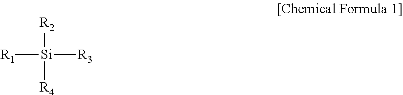
[0007]One purpose of the present disclosure is to provide an etching solution for a silicon substrate in which an etching selectivity of a silicon nitride film relative to a silicon oxide film may be improved by increasing a concentration of a silane compound (silicon) in the etching solution for the silicon substrate to lower an etching rate of the silicon oxide film.
[0008]Further, another purpose of the present disclosure is to provide an etching solution for a silicon substrate that may prevent formation of silicon-based particles or prevent an etching rate of the silicon nitride film from being lowered.
[0017]The silicon additive in the etching solution for the silicon substrate according to the present disclosure may increase a concentration of the silane compound (e.g., silicic acid) under an etching condition of the silicon substrate, thereby to lower the etching rate of the silicon oxide film.
[0019]Further, the aryl group bonded to the silicon atom maintains stable binding with the silicon atom at room temperature, thereby preventing the concentration of the silane compound (silicon) in the etching solution for the silicon substrate from increasing dramatically, thereby to prevent the etching rate of the silicon nitride film from being lowered.
Problems solved by technology
However, the dry etching method is much inferior to the wet etching method in terms of productivity and economy.
Thus, various defects and pattern abnormalities may occur.
Method used
View moreImage
Smart ImageViewing Examples


Examples
example 1
Present Example 1
[0084]An etching solution for a silicon substrate was prepared by mixing phosphoric acid 85 wt %, silicon additive 1,000 ppm represented by a following Chemical Formula 3, and water as remainder:
[0085]
example 2
Present Example 2
[0086]An etching solution for a silicon substrate was prepared in the same manner as in Present Example 1 except that silicon additive represented by a following Chemical Formula 4 was used:
[0087]
example 3
Present Example 3
[0088]An etching solution for a silicon substrate was prepared in the same manner as in Present Example 1 except that silicon additive represented by a following Chemical Formula 5 was used:
[0089]
Login to View More PUM
| Property | Measurement | Unit |
|---|---|---|
| pH | aaaaa | aaaaa |
| concentration | aaaaa | aaaaa |
| hydrophilic | aaaaa | aaaaa |
Abstract
Disclosed is an etching solution for a silicon substrate. More specifically, an etching solution for a silicon substrate is disclosed in which a concentration of a silane compound (silicon) in the etching solution for the silicon substrate is adjusted to improve an etching selectivity of a silicon nitride film relative to a silicon oxide film during etching of the nitride film.
Description
CROSS TO REFERENCE TO RELATED APPLICATIONS[0001]This application claims the priority of Korean Patent Application No. 10-2019-0010297 filed on Jan. 28, 2019, in the Korean Intellectual Property Office, the disclosure of which is hereby incorporated by reference in its entirety.BACKGROUND1. Technical Field[0002]The present disclosure relates to an etching solution for a silicon substrate, and a method for manufacturing a semiconductor device using the etching solution. More specifically, the present disclosure relates to an etching solution for a silicon substrate, and a method for manufacturing a semiconductor device using the etching solution, in which an etching selectivity of a silicon nitride film relative to a silicon oxide film while etching the silicon nitride film may be improved by adjusting a concentration of a silane compound (e.g., silicic acid) in the etching solution for the silicon substrate.2. Description of the Related Art[0003]Currently, there are various methods o...
Claims
Login to View More Application Information
Patent Timeline
 Patent Type & AuthorityPatents(United States)
IPC IPC(8): C08K13/06H01L21/465C09K13/06
CPCC09K13/06H01L21/465H01L21/30604C09K13/08H01L21/31111Y02P70/50
InventorYOO, HO-SEONGKIM, MYUNG-HYUNLEE, JUN-EUNJANG, PYONG-HWA
OwnerOCI