HTO (high temperature oxide) deposition for capacitor dielectrics

Inactive Publication Date: 2001-04-17
IBM CORP
View PDF9 Cites 18 Cited by
  • Summary
  • Abstract
  • Description
  • Claims
  • Application Information

AI Technical Summary

Problems solved by technology

Several problems however exist with dielectrics that are formed by ozone TEOS deposition.
For instance, dielectrics that are formed from ozone TEOS are typically thick (200 .ANG.or more) and it is difficult to control the uniformity and repeatability of the thickness using such a deposition process.
Under such conditions, and if deposited directly on silicon, interfacial layers form which may degrade device performance.
In addition, grain boundary leakage paths and lowered barrier heights may result which could lead to high device leakage.
Thus, HTOs formed from prior art LPCVD processes are not reliable enough for use in the current generation of semiconductor devices, nor will they be reliable in future generations either.
In addition, processing with LPCVD

Method used


Image

  • HTO (high temperature oxide) deposition for capacitor dielectrics
  • HTO (high temperature oxide) deposition for capacitor dielectrics

Examples


Embodiment Construction

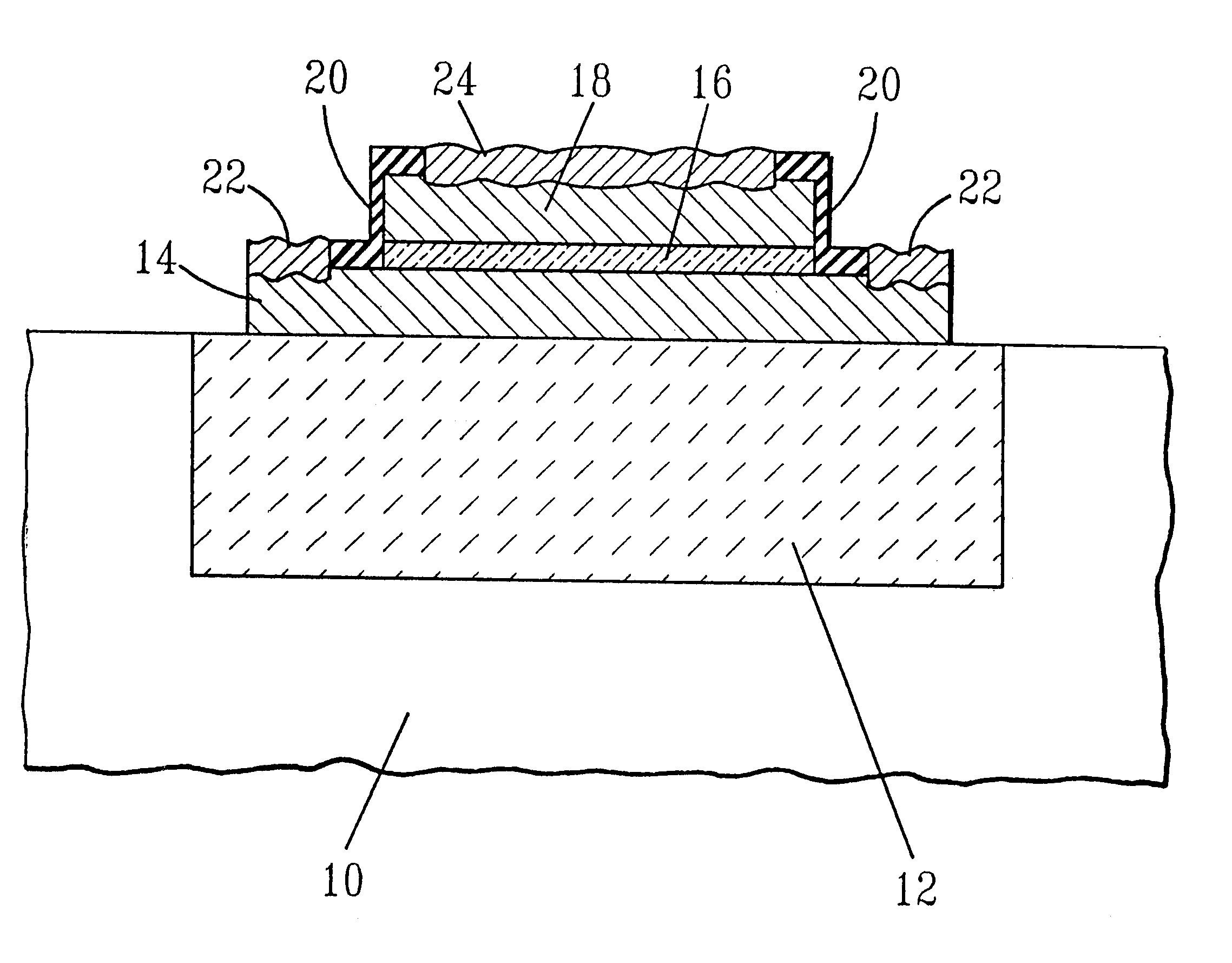
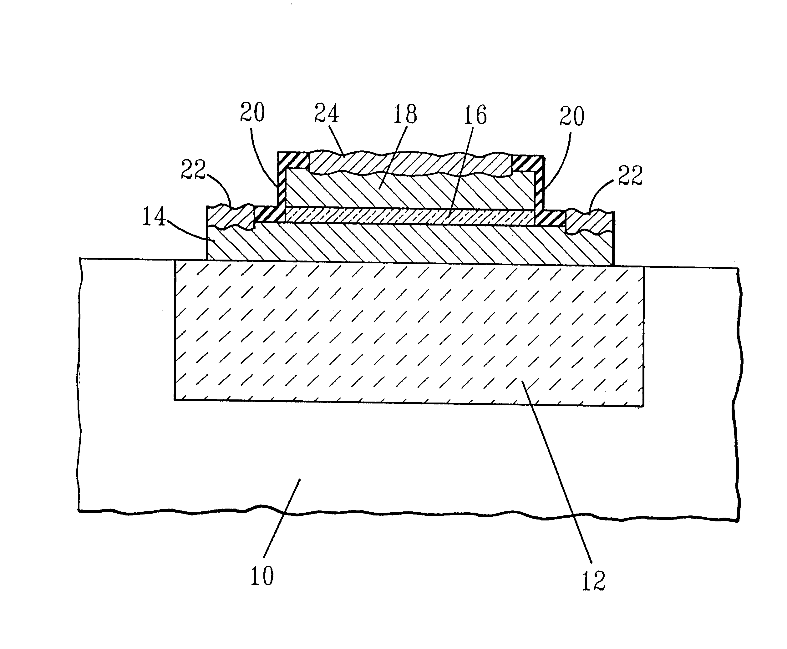
In this example, a capacitor device like the one illustrated in FIG. 1 containing a HTO dielectric of the present invention was prepared and a comparative device containing ozone TEOS was also fabricated. The ozone TEOS containing device was prepared in accordance with prior art methods that are well known to those skilled in the art.

A third device containing a stack of TEOS and the HTO oxide of the present invention was also prepared utilizing prior art processes and the process of the present invention.

In regard to the devices containing the HTO dielectric of the present invention, the devices were fabricated utilizing standard capacitor fabrication processing steps with the exception of the HTO dielectric which was prepared in accordance with the RTCVD process of the present invention. Specifically, the HTO dielectric was formed as follows:

Chamber susceptor temperature: 775.degree. C.

Deposition temperature: 775.degree. C.

Pressure: 75 Torr

Carrier gas conditions:

Main N.sub.2 flow: ...


PUM


Abstract

Reliable HTO (High Temperature Oxide) dielectrics are provide by a rapid thermal chemical vapor deposition (RTCVD) process in which a low pressure and a high ratio of reactants, e.g., oxygen-containing gas to silane-containing gas, is employed. Specifically, the reliable HTO is formed by a rapid thermal chemical vapor deposition at temperatures of from about 500° C. or above, said rapid thermal chemical vapor deposition process being carried out at a pressure of less than 80 Torr and in the presence of at least one oxygen-containing reactant and at least one silane-containing reactant, said reactants having a ratio of oxygen-containing to silane-containing of about 25:1 or greater. Semiconductor devices such as capacitors and transistors that include at least a layer of the high temperature oxide of the present invention used as a dielectric material are also provided.

Description

DESCRIPTION1. Field of the InventionThe present invention is directed to a method for forming a reliable high temperature oxide (HTO) which is useful as a dielectric material in various semiconductor devices such as capacitors, transistors and other like devices which require at least one dielectric material therein. The present invention also relates to various semiconductor devices such as capacitors and transistors which include at least the high temperature oxide of the present invention as a dielectric material.2. Background of the InventionDielectric materials in high density circuits appear as capacitors in dynamic random access memory (DRAM) applications, gate dielectrics in transistors and as decoupling capacitors. The dielectric material in these structures is typically silicon dioxide (SiO.sub.2) which is formed by ozone deposition of tetraethylorthosilicate (TEOS).Several problems however exist with dielectrics that are formed by ozone TEOS deposition. For instance, diel...

Claims


Application Information

Patent Timeline
IPC IPC(8): H01L21/02H01L21/316H01L21/70H01L21/8242
CPCH01L21/02164H01L21/02211H01L21/02271H01L21/31612H01L28/40H01L27/1085H10B12/03
Inventor BALLAMINE, ARNE WATSONCHAN, KEVIN K.COOLBAUGH, DOUGLAS DUANEJOHNSON, DONNA KAYE
Owner IBM CORP
Why Eureka
Try Eureka