Semiconductor device and method of manufacturing semiconductor device
a semiconductor and semiconductor technology, applied in the direction of semiconductor devices, instruments, electrical devices, etc., can solve problems such as draining and deterioration, and achieve the effect of not increasing the number of manufacturing steps
- Summary
- Abstract
- Description
- Claims
- Application Information
AI Technical Summary
Benefits of technology
Problems solved by technology
Method used
Image
Examples
embodiment
[0045](Overall Configuration Example of Display Apparatus)
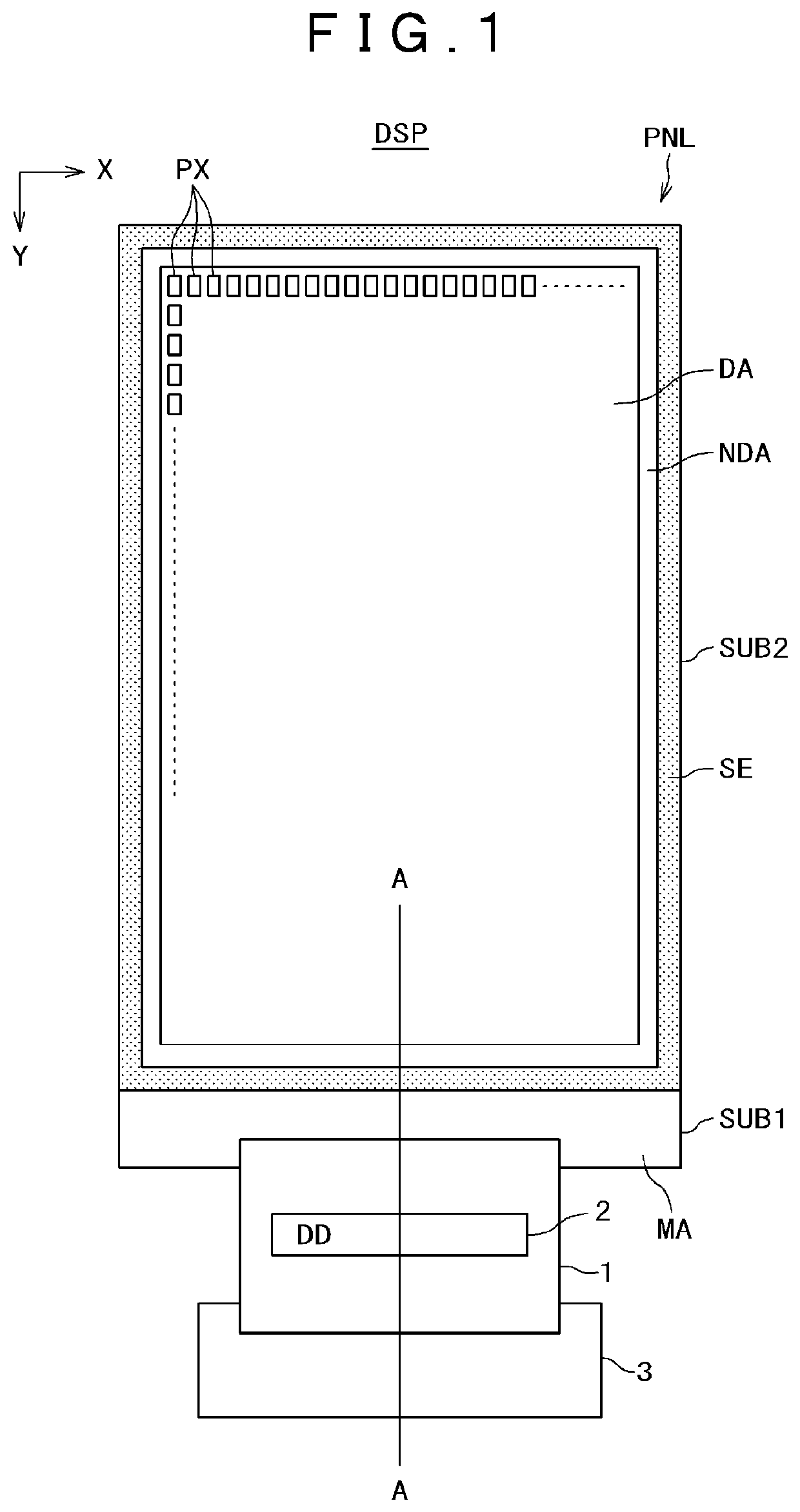
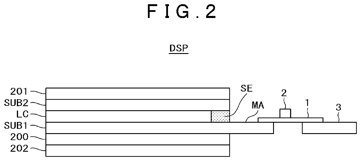
[0046]FIG. 1 is a plan view illustrating one example of an external appearance of a display apparatus according to one embodiment of the present invention. FIG. 2 is a sectional diagram taken along the A-A line in FIG. 1.
[0047]In FIG. 1 and FIG. 2, a display apparatus DSP includes a display panel PNL, a flexible printed circuit board 1, an IC chip 2 and a circuit board 3. The display panel PNL is a liquid crystal display panel and includes a first substrate (also called a TFT substrate or an array substrate) SUB1, a second substrate (also called a counter substrate) SUB2, a liquid crystal layer LC, and a seal SE.
[0048]The display panel PNL includes a display section (a display area) DA which displays an image and a frame-shaped non-display section (non-display area) NDA which surrounds an outer periphery of the display section DA. The second substrate SUB2 confronts the first substrate SUB1. The first substrate SUB1 has a mou...
modified example
[0100]The semiconductor device 10 which has the LTPSTFT and the OSTFT and is used in a display apparatus and so forth is described in the abovementioned embodiment. In the following modified example, a semiconductor device 10a which has only OSTFT and is used in the display apparatus and so forth will be described. In this case, in the configuration of OSTFT which is illustrated in FIG. 4, it is possible to eliminate the metal layers 111 for protection which are connected to the drain region 1092 and the source region 1093. Accordingly, since it is possible to eliminate the film deposition step and the patterning step for the metal layers 111 and the contact hole cleaning step, it becomes possible to reduce the number of manufacturing steps.
[0101]FIG. 19 to FIG. 23 are sectional diagrams illustrating examples of the respective manufacturing steps of the semiconductor device 10a according to the modified example respectively. As illustrated in FIG. 23, the semiconductor device 10a is...
PUM
| Property | Measurement | Unit |
|---|---|---|
| thickness | aaaaa | aaaaa |
| thickness | aaaaa | aaaaa |
| thickness | aaaaa | aaaaa |
Abstract
Description
Claims
Application Information


