
Semiconductor integrated circuit device and method of manufacturing the same

a technology of integrated circuit and semiconductor, which is applied in the direction of semiconductor devices, diodes, electrical apparatus, etc., can solve the problems of gate oxide film not being able to provide stable capacitance and noticeably increasing leakage current, so as to reduce leakage current of capacitive elements constituted by misfet, high threshold voltage, and operation reliably

Inactive Publication Date: 2002-09-19
RENESAS ELECTRONICS CORP
View PDF0 Cites 1 Cited by
  • Summary
  • Abstract
  • Description
  • Claims
  • Application Information

AI Technical Summary

Benefits of technology

[0007] Accordingly, an object of the present invention is to provide a technique of reducing the leakage current in a capacitive element that comprises the gate oxide film of a MISFET.
[0008] Another object of the invention is to provide a technique of forming a capacitive element having a small leakage current, without increasing the number of manufacturing steps.
[0017] Hence, the leakage current of the capacitive element constituted by a MISFET can be decreased since the MISFET has a thick gate insulating film.
[0018] Further, the capacitive element can have a high threshold voltage, because it is constituted by a p-channel MISFET having a gate electrode including an n-type silicon film. The capacitive element can therefore operate reliably even at a low power-supply voltage. In addition, special manufacturing steps need not be performed to increase the threshold voltage of the p-channel MISFET.

Problems solved by technology

If the gate oxide film thickness continues to decrease, however, the leakage current will noticeably increase due to the defects in the gate oxide film or directly due to the tunnel current.
Consequently, the gate oxide film may not be able to provide stable capacitance if used as a capacitive element.

Method used


Image

  • Semiconductor integrated circuit device and method of manufacturing the same
  • Semiconductor integrated circuit device and method of manufacturing the same
  • Semiconductor integrated circuit device and method of manufacturing the same

Examples


embodiment 1

[0050] (Embodiment 1)

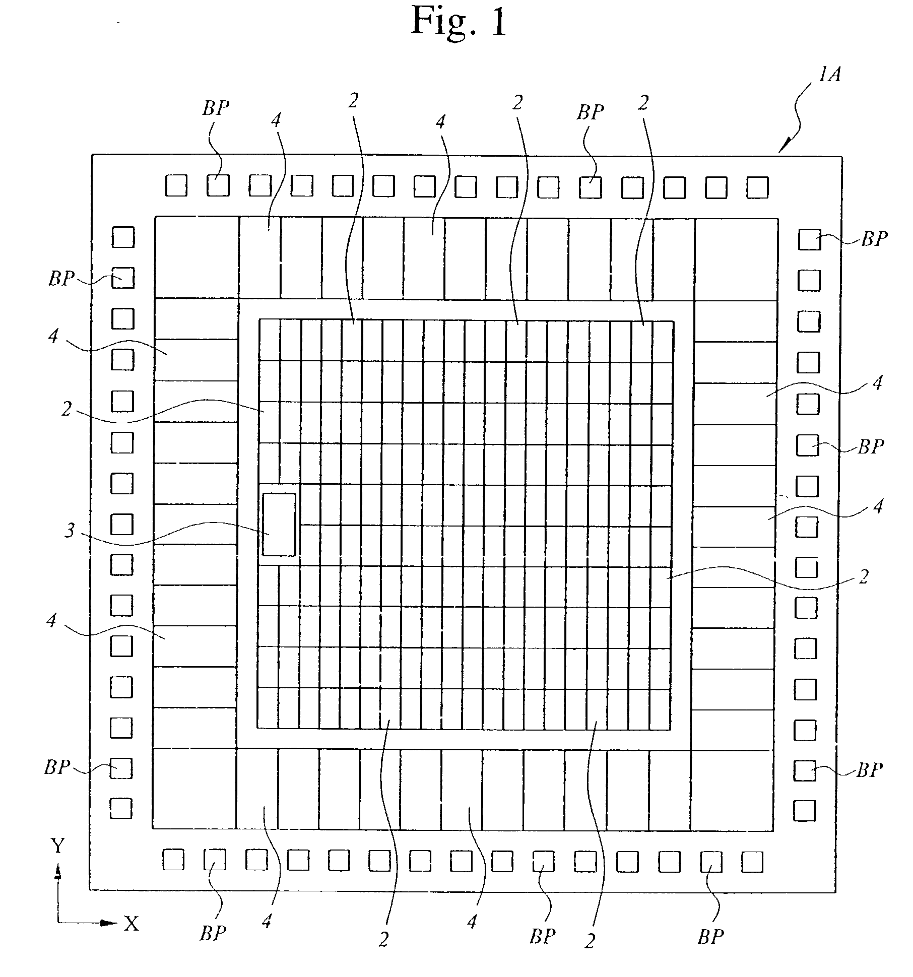
[0051] The semiconductor integrated circuit according to Embodiment 1 is a CMOS (Complementary Metal Oxide Semiconductor) gate array. FIG. 1 shows the semiconductor chip IA incorporating the CMOS gate array.

[0052] As shown in FIG. 1, a number of fundamental cells 2 constituting the logic section of the CMOS gate array are arranged on the center part of the major surface of the semiconductor chip 1A made of single crystal silicon. More specifically, the cells 2 are arranged in rows (in X direction) and columns (in Y direction), forming a matrix. Each fundamental cell 2 is composed of n-channel MISFETs Qn.sub.1 (not shown) and p-channel MISFETs Qp.sub.1 (not shown). The MISFETs Qn.sub.1, and Qp.sub.1 are connected in each cell 2, and the cells 2 are connected to each other based on a logical design. Therefore, the CMOS gate array performs desired logic operations.

[0053] The connection for performing the above logic operations are made by means of a DA (Design Auto...

embodiment 2

[0087] (Embodiment 2)

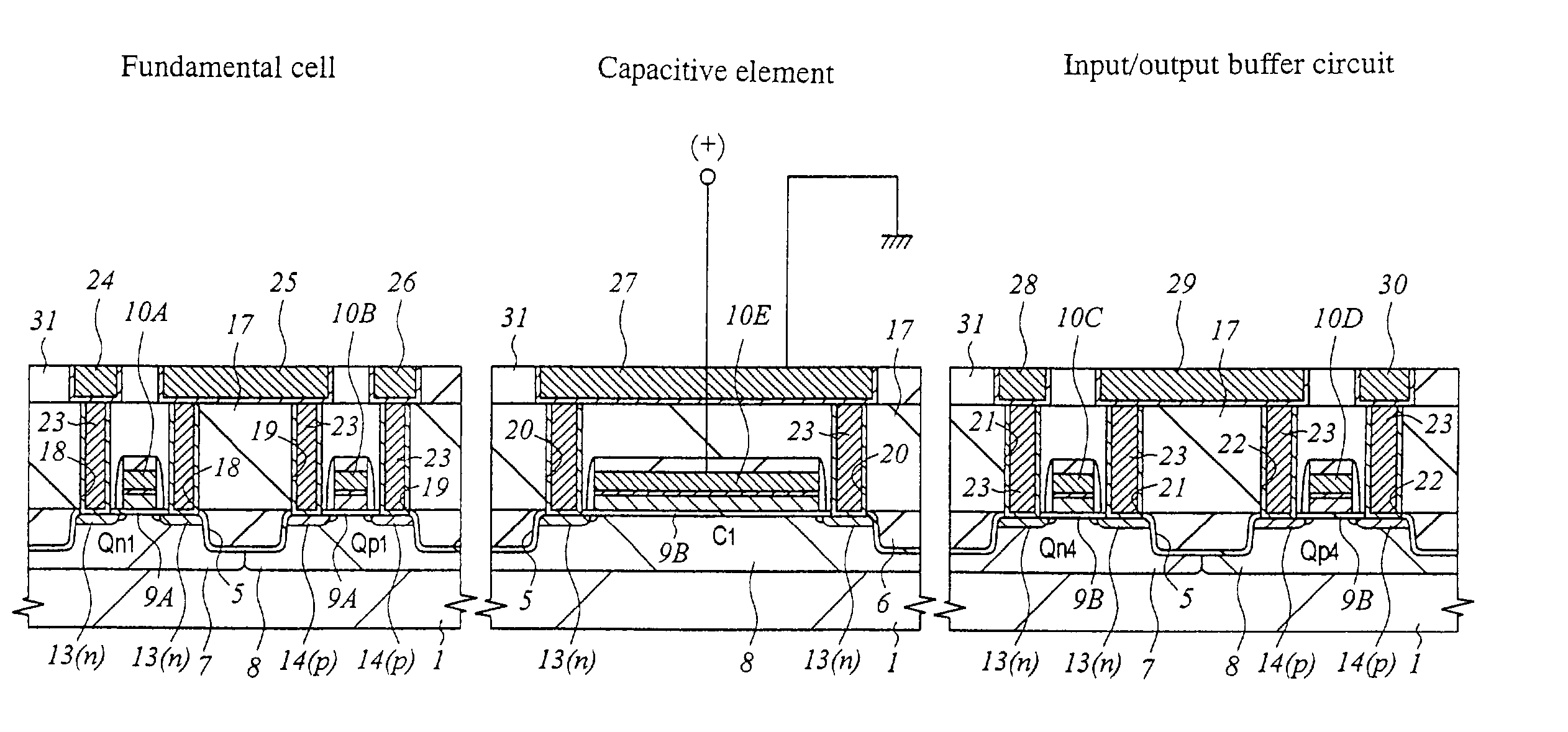
[0088] The capacitive element C.sub.1 provided in the PLL circuit 3 may comprise such an n-channel MISFET as illustrated in FIG. 20. The capacitive element C.sub.1 shown in FIG. 20 is formed in a p-type well 7 of a substrate 1. This capacitive element C.sub.1 is composed of mainly a gate oxide film 9B, a gate electrode 10E, and n-type semiconductor region 13.

[0089] The oxide film 9B of the capacitive element C.sub.1 is as thick as the gate oxide films 9B of MISFETs (Qn.sub.4, QP.sub.4) constituting an input / output buffer circuit 4. That is, it is, for example, about 6.5 nm thick. The p-type well 7 is doped with n-type impurities (e.g., As) so that the n-channel MISFETs have a lower threshold voltage than the other n-channel MISFET Qn.sub.4. Hence, the capacitive element C.sub.1 can reliably operate even at a low power-supply voltage.

[0090] FIG. 21 is a graph illustrating the Vg-C characteristic of the capacitive element C.sub.1 comprising an n-channel MISFET.

[00...

embodiment 3

[0100] (Embodiment 3)

[0101] Embodiments 1 and 2 described above are CMOS gate arrays. Nevertheless, the present invention can be applied to such an LSI of standard-cell system as shown in FIG. 26, designed for a particular use and having macro cells such a logic block, a DRAM (Dynamic Random Access Memory) and a SRAM (Static Random Access Memory). In this case, too, the capacitive elements incorporated in an analog PLL circuit may have gate oxide films 9B that are as thick as the gate oxide films of the MISFETs that constitute an input / output buffer circuit 4 and the gate oxide films of the MISFETs Q.sub.M and Q.sub.S that constitute the memory cells of the DRAM and SRAM. Thus, the same advantages can be attained as in Embodiment 1.

[0102] The present invention can be applied to not only gate arrays and standard cells, but also to various types of LSIs, such as a microcomputer, which has circuits each composed of two or more kinds of MISFETs that differ in the thickness of gate oxide...


PUM


Abstract

A capacitive element C.sub.1 having a small leakage current is formed by utilizing a gate oxide film 9B thicker than that of a MISFET of a logic section incorporated in a CMOS gate array, without increasing the number of steps of manufacturing the CMOS gate array. The capacitive element C.sub.1 has a gate electrode 10E. A part of the gate electrode 10E is made of a polycrystalline silicon film. The polycrystalline silicon film is doped with n-type impurities, so that the capacitive element may reliably operate even at a low power-supply voltage.

Description

[0001] This application is a continuation of U.S. application Ser. No. 09 / 661,372 filed on Sep. 13, 2000, the entire disclosure of which is hereby incorporated by reference.TECHNICAL FIELD OF THE INVENTION[0002] The present invention relates to a semiconductor integrated circuit device and a method of manufacturing the same. More particularly, the invention relates to a technique that is effective and useful when applied to a semiconductor integrated circuit device that has capacitive elements, each comprising a MISFET (Metal Insulator Semiconductor Field Effect Transistor).BACKGROUND OF THE INVENTION[0003] A method is known in which capacitive elements are formed in an LSI comprising MISFETS that compose circuits, by utilizing the gate oxide films of the MISFETS. To use the capacitance of the gate oxide film of each MISFET, the storage region of a p-channel MISFET or the inversion region of an n-channel MISFET is utilized.[0004] The Japanese Patent Application Laid-open Publication...

Claims


Application Information

Patent Timeline
Patent Type & Authority Applications(United States)
IPC IPC(8): H01L27/04H01L21/822H01L21/8234H01L21/8238H01L27/06H01L27/092H10B10/00H10B12/00
CPCH01L27/0629Y10S438/981H01L21/823462H01L27/0733
Inventor SUZUKI, KAZUHISATAKAHASHI, TOSHIROYANAGISAWA, YASUNOBUNONAKA, YUSUKE
Owner RENESAS ELECTRONICS CORP
Learn More