Semiconductor device and method of manufacturing the semiconductor device
a semiconductor and semiconductor technology, applied in the direction of semiconductor devices, electrical appliances, transistors, etc., can solve the problems of unavoidable further fluctuations in many transistor characteristics, difficult to perform precise control, and fluctuation of drain resistance layer, etc., to achieve the desired fine dimension, low cost, and sufficient element characteristics
- Summary
- Abstract
- Description
- Claims
- Application Information
AI Technical Summary
Benefits of technology
Problems solved by technology
Method used
Image
Examples
first embodiment
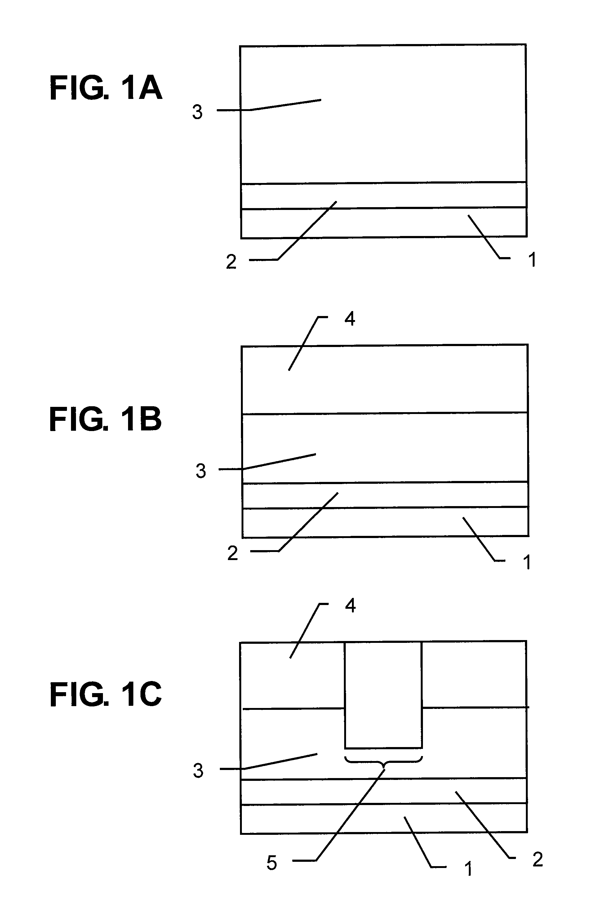
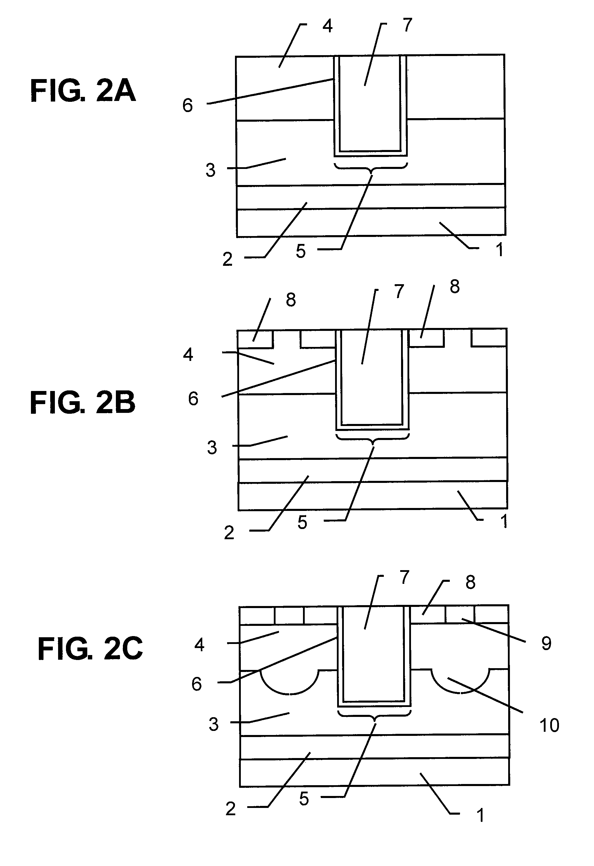
[0025]FIGS. 1A to 1C and 2A to 2C are views illustrating a method of manufacturing a semiconductor device according to the present invention.
[0026]Manufacturing steps for a trench MOSFET according to the present invention are described in order along with the drawings.
[0027]First, as illustrated in FIG. 1A, on an N+ type buried layer 2 formed on a P type semiconductor substrate 1, an epi layer 3 is provided, and the epi layer 3 is entirely doped with N type impurities (here, called as N-epi layer 3). The N+ type buried layer 2 is formed by doping of antimony (Sb), arsenic (As), or phosphorus (P) to have a concentration of 5×1017 cm−3 to 5×1019 cm−3. Further, the N-epi layer 3 is realized by doping of phosphorus to have a concentration of 1×1015 cm−3 to 5×1017 cm−3. The thicknesses of the N+ type buried layer 2 and the N-epi layer 3 are about 2 μm to 10 μm and 2 μm to 10 μm, respectively.
[0028]Then, shallow trench isolation (STI) for element isolation is formed in the N-epi layer 3, ...
second embodiment
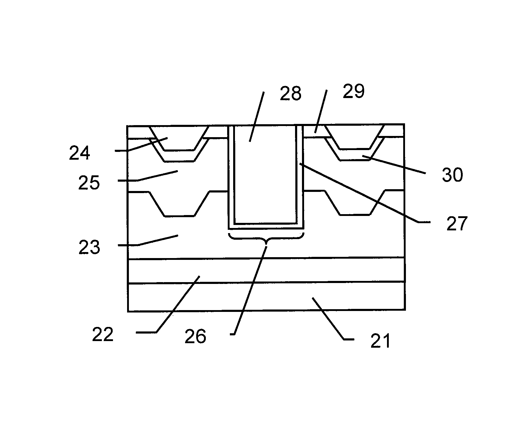
[0038]FIGS. 3A to 3C and 4A and 4B are views illustrating a method of manufacturing a semiconductor device according to the present invention.
[0039]First, as illustrated in FIG. 3A, on an N+ type buried layer 22 formed on a P type semiconductor substrate 21, an epi layer 23 is provided, and the epi layer 23 is entirely doped with N type impurities (here, called as N-epi layer 23). The N+ type buried layer 22 is formed by being doped with antimony (Sb), arsenic (As), or phosphorus (P) to have a concentration of 5×1017 cm−3 to 5×1019 cm−3. Further, the N-epi layer 23 is realized by being doped with phosphorus to have a concentration of 1×1015 cm−3 to 5×1017 cm−3. The thicknesses of the N+ type buried layer 22 and the N-epi layer 23 are about 2 μm to 10 μm and 2 μm to 10 μm, respectively.
[0040]Next, an STI (called as shallow trench 24) for element isolation is formed in the N-epi layer 23, and an insulating film is filled in the shallow trench 24. After that, the insulating film in the...
PUM
 Abstract
Description
Claims
Application Information


