Semiconductor device and manufacturing method thereof

a semiconductor and semiconductor technology, applied in the direction of transistors, optics, instruments, etc., can solve the problems of sudden increase in off current, and inability to conduct moving picture display for images with an enormous amount of information for high definition display, so as to reduce manufacturing costs, reduce leak current, and simplify the tft manufacturing process

Inactive Publication Date: 2007-10-18
SEMICON ENERGY LAB CO LTD +1
View PDF7 Cites 0 Cited by
  • Summary
  • Abstract
  • Description
  • Claims
  • Application Information

AI Technical Summary

Benefits of technology

[0027] When the present invention is applied, the gettering regions formed in the semiconductor layers in the n-channel TFT and the p-channel TFT are produced by steps of adding the impurity element for imparting the n-type and the impurity element for imparting the p-type. Thus, an additional step for gettering is completely unnecessary so that a TFT manufacturing process can be simplified and a manufacturing cost can be reduced. Further, as to a catalytic element gettering step used in a semiconductor film crystallization step, the gettering efficiencies in the n-channel TFT and the p-channel TFT can be made equal. Furthermore, the catalytic elements can be sufficiently moved to the gettering region so as not to segregate in the channel forming region and the junction portion between the channel forming region and the source region or the drain region.
[0028] Therefore, the occurrence of a leak current resulting from the segregation of catalytic elements can be suppressed. In particular, when used as a switching element in a pixel portion, TFTs with satisfactory characteristics can be realized.
[0029] Also, a semiconductor film for which crystallization using a catalytic element is performed indicates satisfactory crystallinity. Thus, even when used as elements for a driver circuit for which high field effect mobility is required, the TFTs manufactured according to the present invention can obtain satisfactory characteristics.

Problems solved by technology

Further, if the information is not written for a short time, it is impossible that moving picture display is conducted for images with an enormous amount of information for high definition display.
However, with respect to a TFT manufactured using as a semiconductor layer a crystalline silicon film obtained using a catalytic element without processing, there is a problem in that an off current is suddenly increased.
Thus, it is considered that the segregation of the catalytic elements becomes a current escape path (leakage path) and this causes a sudden increase in off current.
Thus, there is a problem in that a difference is caused between the n-channel TFT and the p-channel TFT with respect to efficiency that catalytic elements uniformly contained in the semiconductor films move to the gettering regions.
It is difficult that an impurity element for imparting a p-type is sufficiently added to the source region or the drain region of the n-channel TFT without increasing the number of steps.
Thus, a difference of concentrations of the impurity elements added to the semiconductor layers of the n-channel TFT and the p-channel TFT relates to a difference of efficiencies that the catalytic element moves to the gettering region so that this becomes a cause of a problem in that a variation in element characteristics is caused.
Thus, there is a problem in that inconveniences related to a TFT element such as an increase in resistivity and a reduction in on current value may be caused.

Method used


Image

  • Semiconductor device and manufacturing method thereof
  • Semiconductor device and manufacturing method thereof
  • Semiconductor device and manufacturing method thereof

Examples


embodiment 1

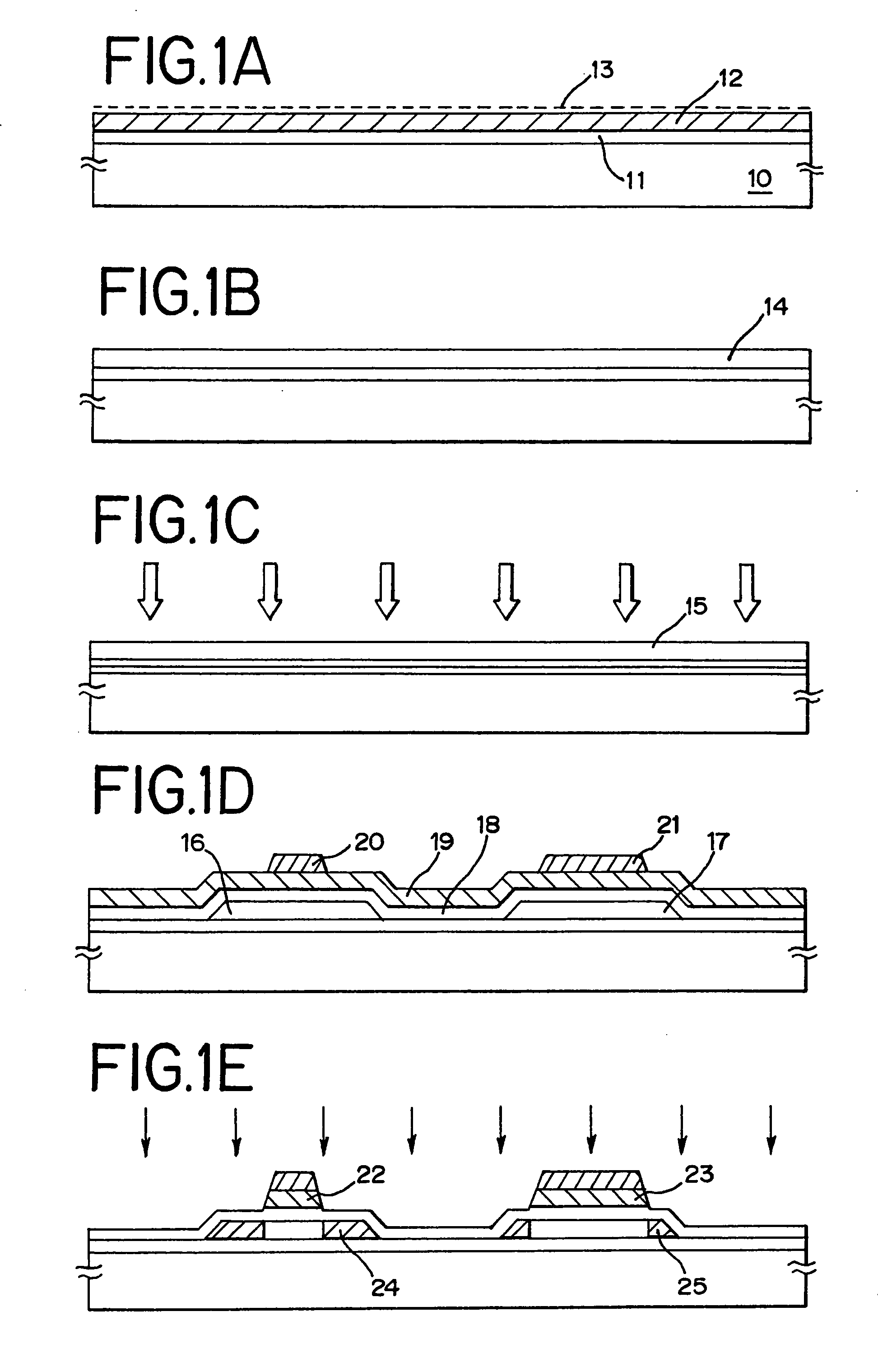
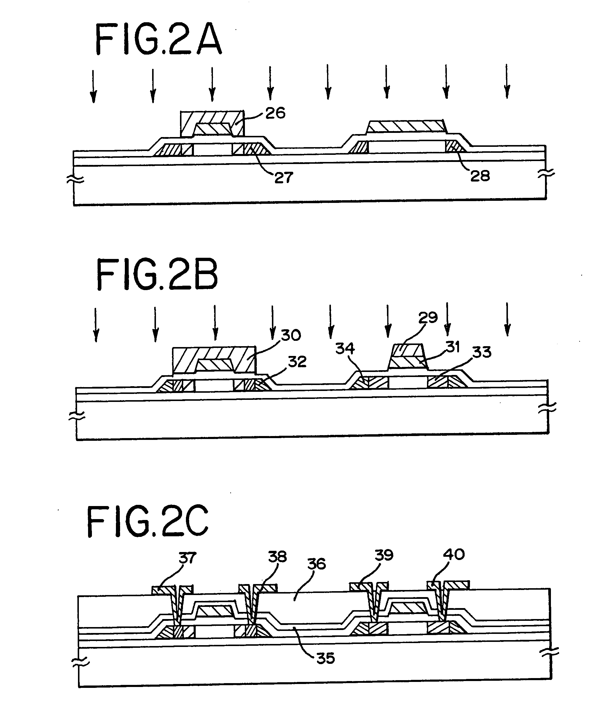
[0063] An embodiment of the present invention will be described with reference to FIGS. 3 to 5 and 11. Here, a detailed description is given step by step on a method of manufacturing, on the same substrate, a pixel TFT for a pixel portion and TFTs for a driving circuit provided in the periphery of the pixel portion.

[0064] In FIG. 3A, a low alkaline glass substrate or a quartz substrate may be used for a substrate 100. This embodiment employs a low alkaline glass substrate. In this case, the substrate may be subjected to heat treatment at a temperature 10 to 20° C. lower than the glass distortion point. On a surface of the substrate 100 on which the TFTs are to be formed is covered with a base film 101 in order to prevent diffusion of impurities from the substrate 100. The base film may be a silicon oxide film, a silicon nitride film, a silicon oxynitride film, or the like. For instance, the base film may be a laminate of a silicon oxynitride film 101a formed from SiH4, NH3, and N2O...

embodiment 2

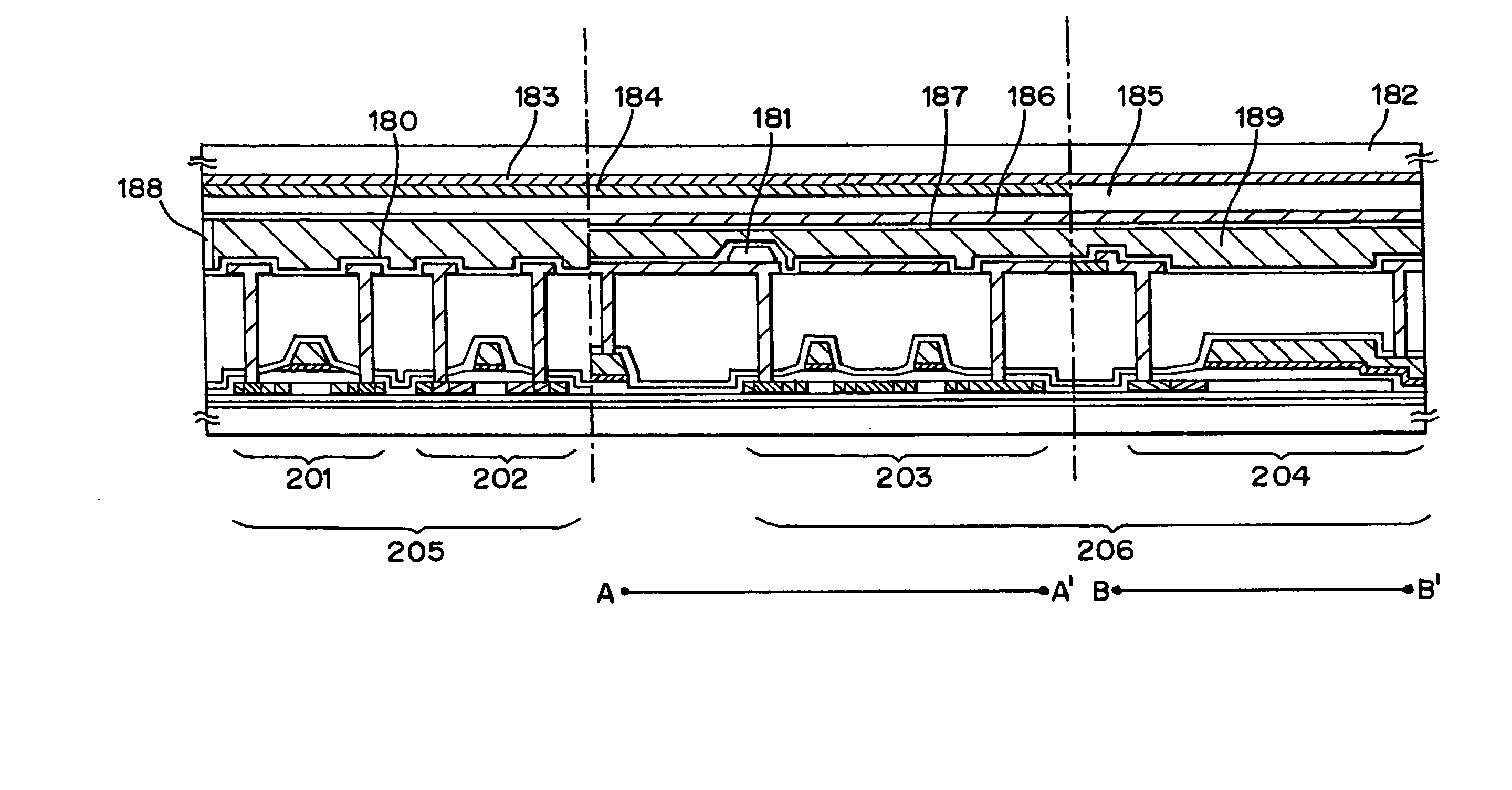
[0106] In this embodiment a process of manufacturing an active matrix liquid crystal display device (also referred to as a liquid crystal display panel) from the active matrix substrate manufactured in Embodiment 1 is described below. FIG. 6 is used for explanation.

[0107] First, in accordance with Embodiment 1, the active matrix substrate in a state shown in FIG. 5B is obtained, and thereafter, an alignment film 180 is formed on the active matrix substrate of FIG. 5B, and is subjected to a rubbing process. Note that, in this embodiment, before the formation of the alignment film 180, a columnar spacer 181 for maintaining a gap between the substrates is formed at a desired position by patterning an organic resin film such as an acrylic resin film. Further, spherical spacers may be scattered on the entire surface of the substrate in place of the columnar spacer.

[0108] Next, an opposing substrate 182 is prepared. On the opposing substrate 182, there are formed a colored layers 183, 1...

embodiment 3

[0115]FIG. 8 is a block diagram of a semiconductor device manufactured in accordance with the present invention. Shown in FIG. 8 is the circuit structure for analog driving. This embodiment describes a semiconductor device having a source side driving circuit 90, a pixel portion 91, and a gate side driving circuit 92. In this specification, the term driving circuit generically refers to a source side driving circuit and a gate side driving circuit.

[0116] The source side driving circuit 90 is provided with a shift register 90a, a buffer 90b, and a sampling circuit (transfer gate) 90c. The gate side driving circuit 92 is provided with a shift register 92a, a level shifter 92b, and a buffer 92c. A level shifter circuit may be provided between the sampling circuit and the shift register if necessary.

[0117] In this embodiment, the pixel portion 91 is composed of a plurality of pixels and each of the plural pixels has a TFT element.

[0118] Though not shown in the drawing, another gate s...


PUM

PropertyMeasurementUnit
thicknessaaaaaaaaaa
thicknessaaaaaaaaaa
wavelengthaaaaaaaaaa

Abstract

A catalytic element is added to an amorphous semiconductor film and heat treatment is conducted therefor to produce a crystalline semiconductor film with good quality, a TFT (semiconductor device) with a satisfactory characteristic is realized using the crystalline semiconductor film. A semiconductor layer includes a region containing an impurity element which has a concentration of 1×10¹⁹/cm3 to 1×10²¹/cm3 and belongs to group 15 of the periodic table and an impurity element which has a concentration of 1.5×10¹⁹/cm3 to 3×10²¹/cm3 and belongs to group 13 of the periodic table, and the region is a region to which a catalytic element left in the semiconductor film (particularly, the channel forming region) moves.

Description

[0001] This application is a divisional of copending U.S. application Ser. No. 10 / 365,911, filed on Feb. 13, 2003.BACKGROUND OF THE INVENTION [0002] 1. Field of the Invention [0003] The present invention relates to a semiconductor device and a method of adding a metallic element having a function for promoting crystallization to an amorphous semiconductor film and conducting heat treatment to form a crystalline semiconductor film, and manufacturing a thin film transistor (TFT) using the crystalline semiconductor film. [0004] 2. Description of the Related Art [0005] A liquid crystal display device in which a pixel portion and a driver circuit are provided on the same substrate is used as a monitor for a personal computer (PC) and further begins to expand into ordinary households. For example, a liquid crystal display instead of a CRT (cathode-ray tube) is introduced as a television into ordinary households. In addition, a front projector for watching a movie or playing a game is intr...

Claims


Application Information

Patent Timeline
Patent Type & Authority Applications(United States)
IPC IPC(8): H01L27/092H01L21/20G02F1/1368H01L21/336H01L21/77H01L21/84H01L27/12H01L29/423H01L29/49H01L29/786
CPCH01L27/12H01L27/1277H01L29/4908H01L29/42384H01L29/786
Inventor NAKAZAWA, MISAKOMAKITA, NAOKI
Owner SEMICON ENERGY LAB CO LTD
Why Eureka
Try Eureka