Organic light-emitting diode, organic light-emitting display including the same, and method of manufacturing the same

a technology of organic light-emitting diodes and light-emitting displays, which is applied in the direction of organic semiconductor devices, solid-state devices, semiconductor devices, etc., can solve the problems of negative influence on performance and lifespan of woled, and the difference in energy level between functional layers constituting blue light-emitting layers, so as to improve the luminous efficacy and lifespan of the woled, improve the operation characteristics and long life, and reduce the operation voltage

Active Publication Date: 2022-04-05
LG DISPLAY CO LTD
View PDF10 Cites 1 Cited by
  • Summary
  • Abstract
  • Description
  • Claims
  • Application Information

AI Technical Summary

Benefits of technology

[0008]An aspect of the present disclosure is to provide an organic light-emitting diode capable of reducing operation voltage while improving luminous efficacy and lifespan thereof, and an organic light-emitting display including the same.
[0009]An aspect of the present disclosure is to provide an organic light-emitting diode that may include a blue light-emitting layer while securing improved operation characteristics and long lifespan.

Problems solved by technology

In a typical white organic light-emitting diode (WOLED), a difference in energy level between functional layers constituting a blue light-emitting layer deteriorates efficiency in injection of electrons or holes at an interface between the functional layers, thereby having a negative influence on performance and lifespan of the WOLED.

Method used


Image

  • Organic light-emitting diode, organic light-emitting display including the same, and method of manufacturing the same
  • Organic light-emitting diode, organic light-emitting display including the same, and method of manufacturing the same
  • Organic light-emitting diode, organic light-emitting display including the same, and method of manufacturing the same

Examples


example 1

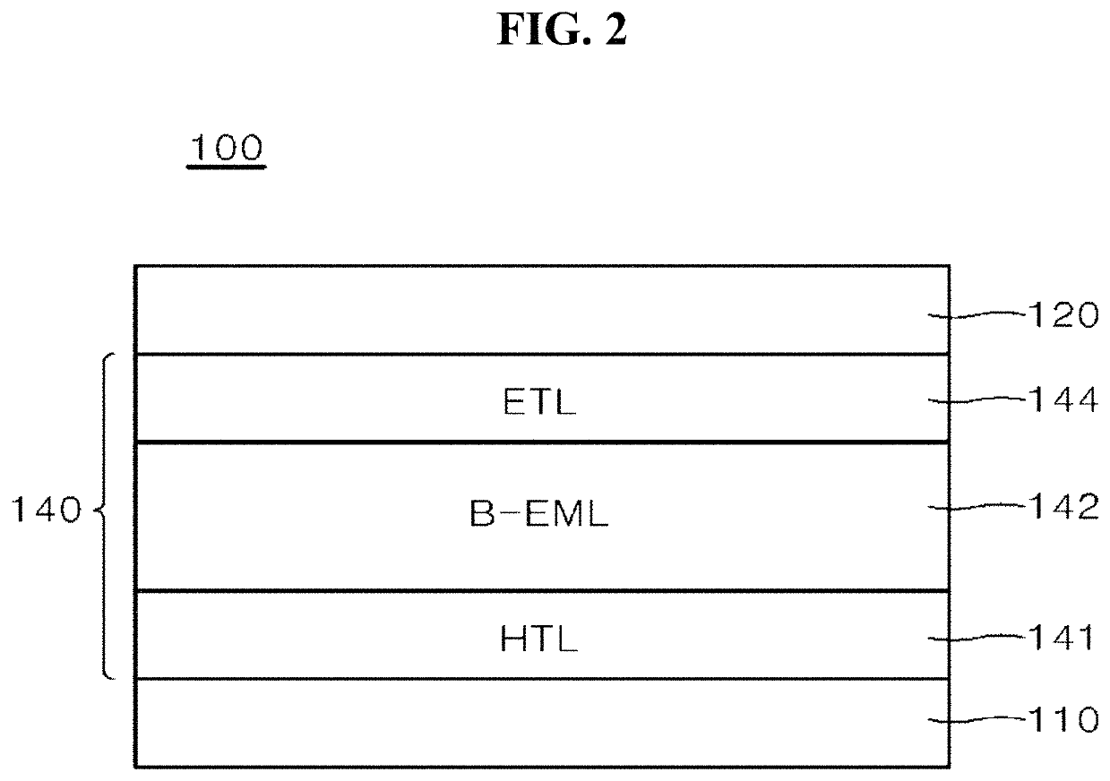
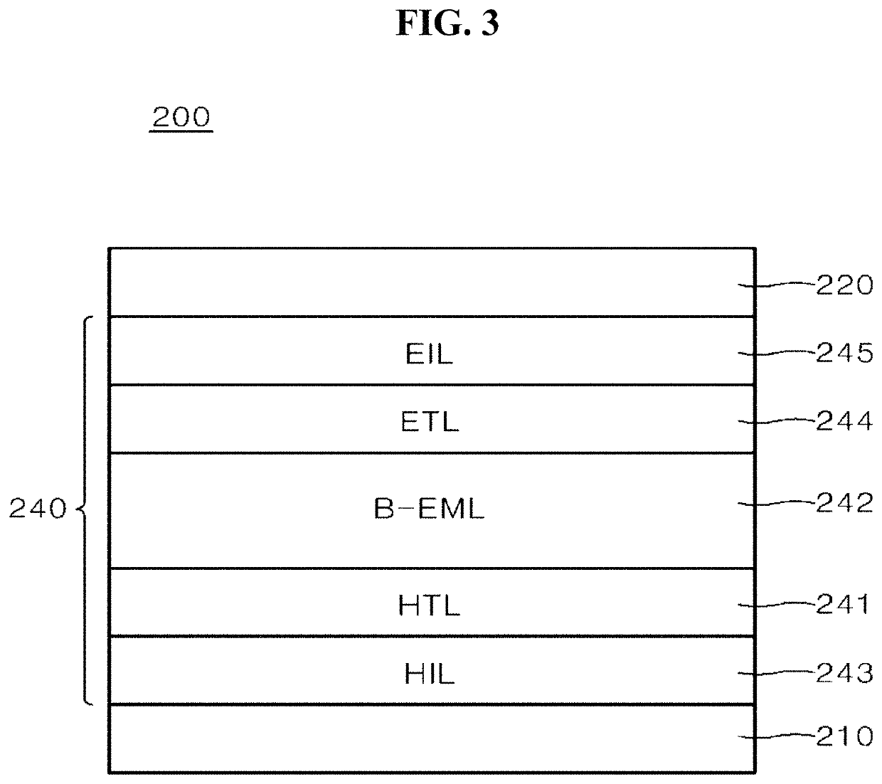
[0098]In a vacuum chamber at a pressure of 5×10⁻⁸ to 7×10⁻⁸ torr, an organic light-emitting diode was fabricated by sequentially depositing a hole injection layer, a hole transport layer (HTL1), a blue light-emitting layer (blue host material (BH) and blue fluorescent dopant material (BD, 4 wt % doping)), an electron transport layer (ETL1), an electron injection layer (LiF) and a cathode on an ITO substrate (anode).

[0099]FIG. 6 is an energy diagram depicting energy levels of an organic light-emitting diode of Example 1.

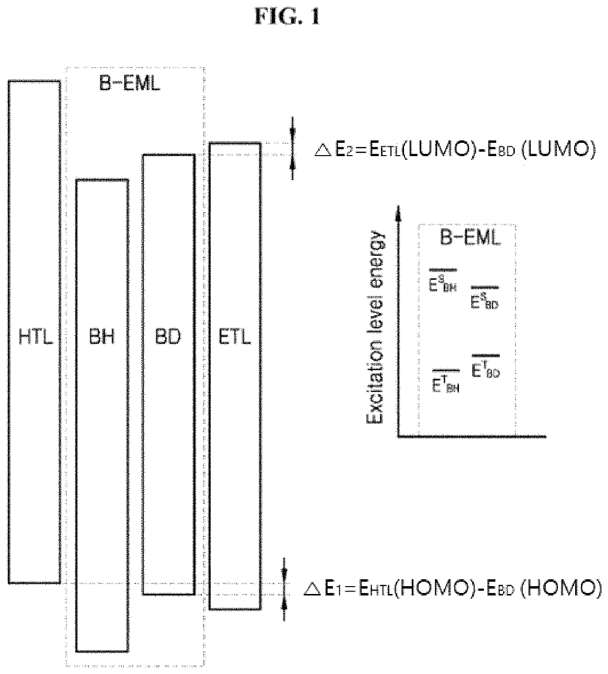
[0100]FIG. 6 is an energy diagram depicting the energy levels of HTL1 / BH+BD / ETL1 of the fabricated organic light-emitting diode. In evaluation of the energy level, it could be seen that, in the fabricated organic light-emitting diode, the difference between the HOMO energy level of HTL1 and the HOMO energy level of BD was 0.1 eV or less and the difference between the LUMO energy level of ETL1 and the LUMO energy level of BD was 0.1 eV or less. With reference to FIG. 6...

experimental example 1

ristics of Organic Light-Emitting Diode (Above)

[0106]Operation characteristics of the organic light-emitting diodes fabricated in Example 1 and Comparative Example 1 were evaluated. Table 1 shows voltage-current density, brightness-current efficiency, brightness-external quantum efficiency (EQE), and lifespan of the organic light-emitting diodes fabricated in Example 1 and Comparative Example 1.

[0107]

TABLE 1Voltage-currentBrightness-externalVoltagedensityquantum efficiencyLifespanItem(V)(Cd / A)(EQE)(hours)Example 13.78.08.150Comparative4.56.06.230Example 1

[0108]The organic light-emitting diode of Comparative Example 1 had a larger difference in HOMO energy level between HTL2 and BH than that of Example 1 and ETL2 had a lower LUMO energy level than BD in Comparative Example 1. As a result, Comparative Example 1 did not satisfy the following conditions:

[0109](F) The hole transport layer material has a higher HOMO energy level than the blue fluorescent dopant material and a difference i...


PUM

PropertyMeasurementUnit
LUMO energy levelaaaaaaaaaa
HOMO energy levelaaaaaaaaaa
thicknessaaaaaaaaaa

Abstract

An organic light-emitting diode includes: a first electrode, a light-emitting stack thereon including, sequentially stacked: a hole transport layer (HTL) including an HTL material, a blue light-emitting layer including: a blue host material (BHM) and a blue fluorescent dopant (BFD) material, and an electron transport layer (ETL) including an ETL material, and a second electrode on the light-emitting stack, wherein the BFD material has a higher LUMO, a higher HOMO, and a lower singlet energy than the BHM, the HTL material has a higher HOMO than the BHM and the BFD material, a difference in HOMO between the HTL material and the BFD material is 0.1 eV or less, the ETL material has a higher LUMO than the BHM and the BFD material, and a difference in LUMO between the ETL material and the BFD material is 0.1 eV or less.

Description

CROSS-REFERENCE TO RELATED APPLICATION(S)[0001]This application claims the benefit of and priority to Korean Patent Application No. 10-2017-0178314, filed on Dec. 22, 2017, the entirety of which is hereby incorporated by reference.BACKGROUND1. Technical Field[0002]The present disclosure relates to an organic light-emitting diode, an organic light-emitting display including the same, and a method of manufacturing the same.2. Discussion of the Related Art[0003]Recently, there is increasing interest in flat-panel display elements occupying a small space, with increasing size of displays. A technology of an organic light-emitting display including organic light-emitting diodes (OLEDs) as the flat-panel display elements has been rapidly developed in the art.[0004]An organic light-emitting diode emits light through conversion of energy of excitons created by pairs of electrons and holes generated upon injection of charges into an organic light-emitting layer formed between an anode and a ...

Claims


Application Information

Patent Timeline
Patent Type & Authority Patents(United States)
IPC IPC(8): H01L51/50H01L51/00H01L51/52H01L27/32
CPCH01L51/5036H01L51/00H01L51/0059H01L51/5004H01L51/5012H01L51/5056H01L51/5072H01L51/5092H01L51/5206H01L51/5221H01L51/5278H01L27/3209H01L2251/308H01L2251/552H10K59/32H10K50/11H10K2101/40H10K50/16H10K50/15H10K50/19H10K2101/30H10K59/38H10K85/615H10K50/12H10K50/125H10K50/14H10K50/81H10K50/82H10K50/171H10K85/631H10K99/00H10K2102/103
Inventor KIM, SANGBEOMSEO, JEONGDAE
Owner LG DISPLAY CO LTD
Why Eureka
Try Eureka