Unlock instant, AI-driven research and patent intelligence for your innovation.

Optical semiconductor device package, optical semiconductor device, and manufacturing method for optical semiconductor device package

a manufacturing method and semiconductor technology, applied in the direction of semiconductor devices, basic electric elements, electrical apparatus, etc., can solve the problems of reducing reducing the life-span of the optical semiconductor device, and exhibiting photocatalytic action, etc., to achieve shorten the life-span, reduce the degree of reflectance, and achieve sufficient emission luminance

Active Publication Date: 2022-05-17
PANASONIC HLDG CORP
View PDF11 Cites 0 Cited by
  • Summary
  • Abstract
  • Description
  • Claims
  • Application Information

AI Technical Summary

Benefits of technology

This configuration effectively inhibits reflectance decrease and extends the lifespan of the device by preventing copper diffusion and silver blackening, maintaining high emission luminance over long-term use.

Problems solved by technology

However, with the silver plating having such a layer structure, there is a problem of a decrease in the degree of reflectance caused by discoloring of the surface of the silver plating into a color of copper, as a result of copper of underlayer metal being diffused to the surface of the silver plating due to the influence of heat generation caused by long-term use of the optical semiconductor device.
However, when the optical semiconductor device is driven for a long period of time, light emitted from the optical semiconductor element irradiates titanium oxide which is a white pigment included in the resin enclosure that functions as a reflector (i.e., reflecting body), causing the titanium oxidize to be excited and exhibit a photocatalytic action.
As a result, active oxygen (more specifically, superoxide anion) is generated which converts silver into silver oxide and causes blackening of silver, posing a new problem that a life-span of the optical semiconductor device is further shortened.

Method used


Image

  • Optical semiconductor device package, optical semiconductor device, and manufacturing method for optical semiconductor device package
  • Optical semiconductor device package, optical semiconductor device, and manufacturing method for optical semiconductor device package
  • Optical semiconductor device package, optical semiconductor device, and manufacturing method for optical semiconductor device package

Examples


Embodiment Construction

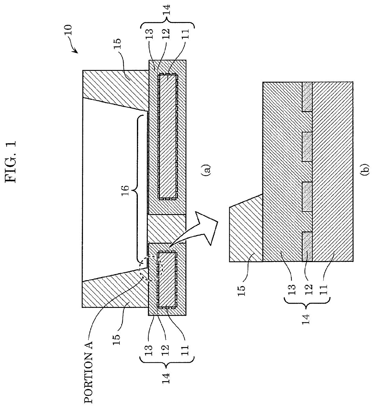
[0022]Hereinafter, an embodiment of the present disclosure will be described with reference to the attached drawings. It should be noted that the present disclosure is not limited to the embodiment and can be implemented with modifications as appropriate within the technical scope of the present discloser. In other words, the embodiment described below indicates one specific example of the present disclosure. The numerical values, shapes, materials, structural components, the arrangement and connection of the structural components, steps, the processing order of the steps, and so on, shown in the following embodiment are mere examples, and therefore do not limit the present disclosure. In addition, among the structural components in the following embodiment, structural components not recited in any one of the independent claims which represent the most generic concept of the present disclosure are described as arbitrary structural components. In addition, each diagram is not necessa...


PUM

PropertyMeasurementUnit
thicknessaaaaaaaaaa
thicknessaaaaaaaaaa
thicknessaaaaaaaaaa

Abstract

An optical semiconductor device package includes a circuit board in which a first metal, a second metal, and a third metal are sequentially stacked in an optical semiconductor element mounting region. The first metal has a first standard electrode potential. The second metal is disposed on a portion of an upper surface of the first metal and has a second standard electrode potential that is greater than the first standard electrode potential. The third metal is disposed on the upper surface of the first metal and an upper surface of the second metal and has a third standard electrode potential that is greater than the first standard electrode potential and less than the second standard electrode potential.

Description

CROSS REFERENCE TO RELATED APPLICATIONS[0001]This application is a U.S. continuation application of PCT International Patent Application Number PCT / JP2018 / 030603 filed on Aug. 20, 2018, claiming the benefit of priority of Japanese Patent Application Number 2017-206258 filed on Oct. 25, 2017, the entire contents of which are hereby incorporated by reference.BACKGROUND1. Technical Field[0002]The present disclosure relates to optical semiconductor device packages, optical semiconductor devices, and manufacturing methods for the optical semiconductor device packages, and in particular to a technique which prevents deterioration of the optical semiconductor device packages when used for a long period of time.2. Description of the Related Art[0003]In conventional optical semiconductor device packages, a silver coating film is provided as a reflective coating film on the outermost layer (i.e., a bottom surface on which an optical semiconductor element is mounted) of a region which is enclo...

Claims


Application Information

Patent Timeline
Patent Type & Authority Patents(United States)
IPC IPC(8): H01L33/60H01L33/00
CPCH01L33/60H01L33/005H01L2933/0058H01L33/62H01L33/486H01L2933/0066
Inventor FUKUNAGA, TAKAHIROKITTAKA, AKINOBU
Owner PANASONIC HLDG CORP
Features
  • R&D
  • Intellectual Property
  • Life Sciences
  • Materials
  • Tech Scout
  • Unparalleled Data Quality
  • Higher Quality Content
  • 60% Fewer Hallucinations
Learn More