Reset method, reset device, and reset system and pixel array using the same
- Summary
- Abstract
- Description
- Claims
- Application Information
AI Technical Summary
Benefits of technology
Problems solved by technology
Method used
Image
Examples
example 1
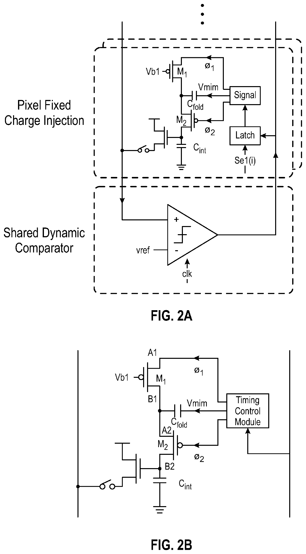
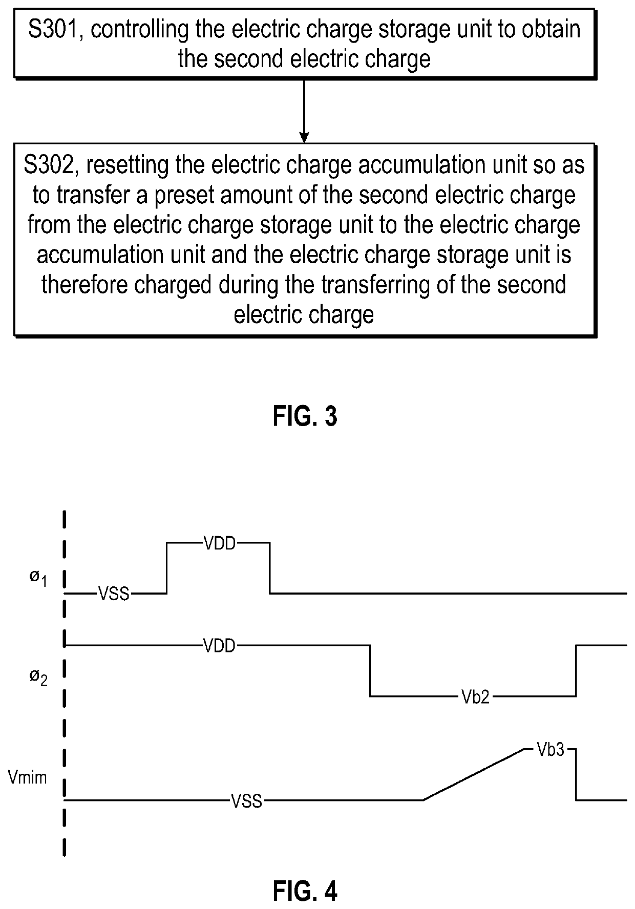
[0075]A detailed electric charge reset process illustrated as follows will be taken as an example to explain each step of the above reset method. FIG. 4 is a timing diagram of the electric charge reset process. A reset circuit structure involved in the electric charge reset process is shown in FIG. 2B. The process is as follows.
[0076]At time 0˜t1, the first signal ϕ1 output from the control module is low electrical level, the second signal ϕ2 is high electrical level, Vmim is low electrical level. In this case, the first switch M1 and the second switch M2 are both turned off.
[0077]At time t1˜t2, the first signal ϕ1 changes to high electrical level, the second signal ϕ2 remains high electrical level, and Vmim remains low electrical level. In this case, the first switch M1 is turned on while the second switch M2 is turned off. When applying the voltage of Vdd to a left plate of the capacitor Cfold in the electric charge storage unit, the first electric charge Q1=−VDD×Cfold.
[0078]At ti...
PUM
 Abstract
Description
Claims
Application Information


