Microfluidic chip and microfluidic device

a microfluidic chip and microfluidic device technology, applied in microstructural devices, microstructural technology, liquid/fluent solid measurement, etc., can solve the problems of large total area of microfluidic chip devices, large number of tubes and connectors, etc., to prevent or reduce the leakage of fluid, prevent or reduce the effect of fluid leakag

Active Publication Date: 2022-10-25
NOK CORP
View PDF21 Cites 0 Cited by
  • Summary
  • Abstract
  • Description
  • Claims
  • Application Information

AI Technical Summary

Benefits of technology

[0011]Accordingly, the present invention provides a microfluidic chip having a simple configuration, enabling the easy formation of different microfluidic devices depending on various applications, and enabling minimizing the area of the formed microfluidic devices, and the present invention provides a microfluidic device including multiple microfluidic chips.
[0013]In accordance with this aspect, the flow passage of the microfluidic chip is formed easily, without using a tube, by combining the flow passage plate and the flat plate. Then, a microfluidic device can be formed by stacking multiple microfluidic chips, each having a different type of flow passage, one on the other, and by aligning the communication hole or the communication through-hole of one microfluidic chip with the communication hole or the communication through-hole of a neighboring microfluidic chip. By changing the laminated microfluidic chips depending on the application, a microfluidic device appropriate to the application can be formed easily. In the formed microfluidic device, each of the microfluidic chips has a different type of flow passage and has a different function. In the formed microfluidic device, multiple flow passages arranged in three dimensions are provided, and these microfluidic chips are stacked in the same two-dimensional region, so that the area of the microfluidic device can be minimized. The annular seal surrounding at least one of the communication hole and the communication through-hole is in contact with, and is compressed by, another microfluidic chip, and this allows flow of fluid between the microfluidic chips while preventing or reducing leakage of the fluid. Accordingly, connectors for connecting the flow passages of multiple microfluidic chips are not necessary.

Problems solved by technology

However, the technique disclosed in Patent Document 2 does not solve the problem of the total area of the microfluidic chip device being large.
Therefore, a large number of tubes and connectors are necessary.

Method used


Image

  • Microfluidic chip and microfluidic device
  • Microfluidic chip and microfluidic device
  • Microfluidic chip and microfluidic device

Examples


Embodiment Construction

[0033]Hereinafter, with reference to the accompanying drawings, multiple embodiments according to the present invention will be described. It is noted that the drawings do not necessarily accurately show relative dimensional ratios of various elements in order that certain features of elements may be exaggerated.

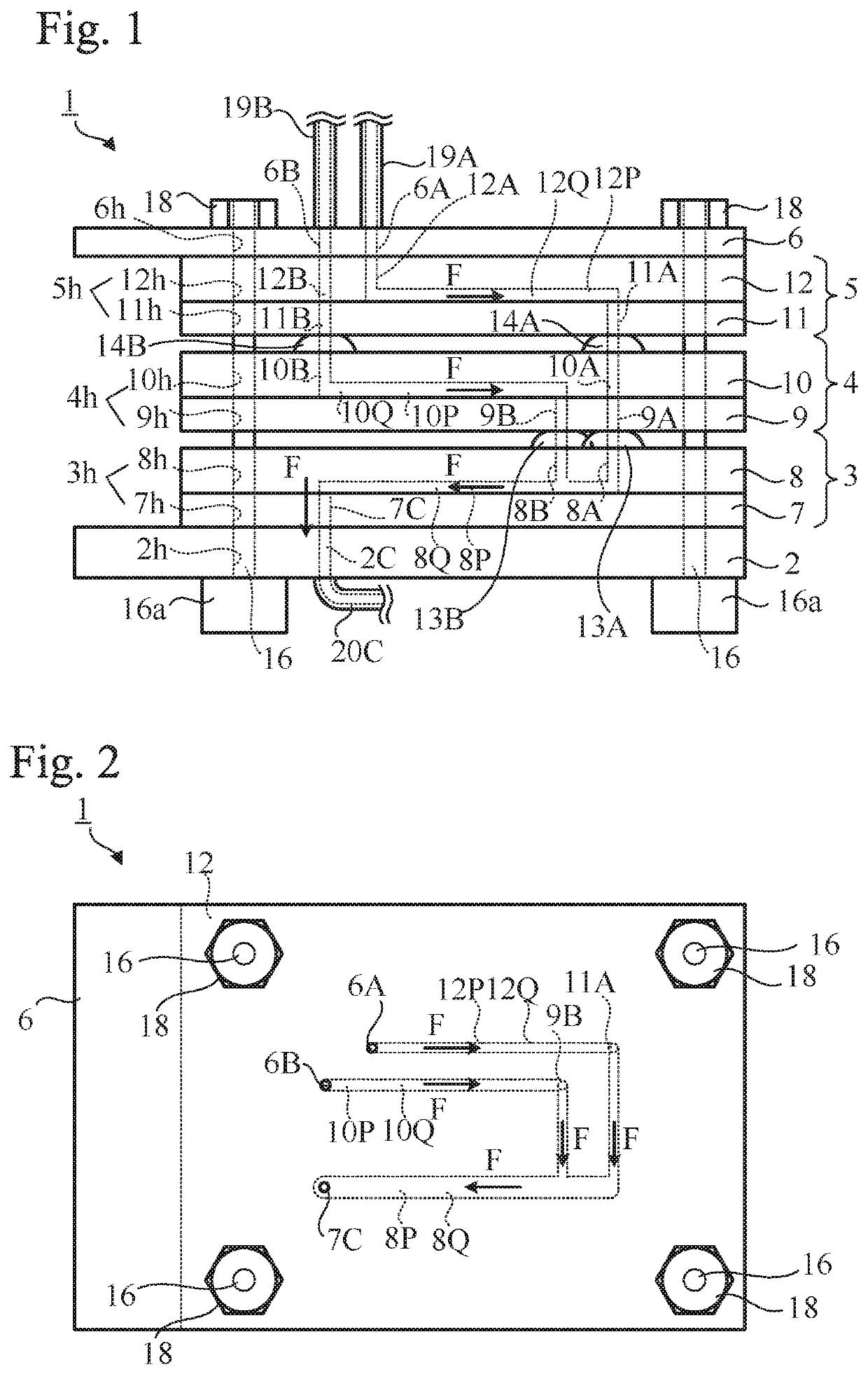
[0034]As shown in FIG. 1, a microfluidic device 1 according to the embodiment has a laminated structure including multiple flat plates stacked one on top of another, more specifically, a supporting flat plate 2, microfluidic chips 3, 4, and 5, and a protection flat plate 6.

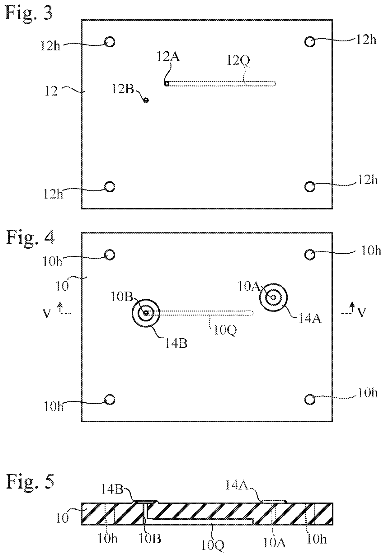
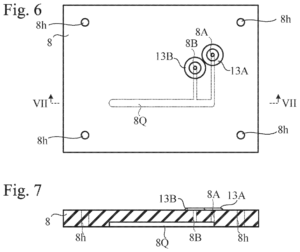
[0035]Each of the microfluidic chips 3, 4, and 5 also has a laminated structure. Specifically, the microfluidic chip 3 includes a flat plate 7 and a flow passage plate 8 that is also a flat plate. The microfluidic chip 4 includes a flat plate 9 and a flow passage plate 10 that is also a flat plate. The microfluidic chip 5 includes a flat plate 11 and a flow passage plate 12 that is also a flat plate.

[0036]...


PUM

PropertyMeasurementUnit
temperatureaaaaaaaaaa
transparentaaaaaaaaaa

Abstract

A microfluidic chip includes a flow passage plate, a flat plate, and an annular seal. In the flow passage plate, a recess forming a flow passage for liquid and a communication hole communicating with the recess are formed. The flat plate is stacked on or under the flow passage plate to close the recess for defining the flow passage. In the flat plate, a communication through-hole communicating with the recess is formed. The annular seal is located on, or formed on, an outer surface of at least one of the flow passage plate and the flat plate, the annular seal surrounding at least one of the communication hole and the communication through-hole. The annular seal is made of an elastomer.

Description

TECHNICAL FIELD[0001]The present invention relates to microfluidic chips and to microfluidic devices.BACKGROUND ART[0002]Microfluidic devices are devices having microminiature flow passages in which liquids flow for analysis or for mixing liquids. In general, flow passages of microfluidic devices are designed to have low Reynolds numbers to allow laminar flow, so that controllability and reproducibility of flow is high. In addition, liquids are treated in microminiature spaces, it is possible to reduce the sizes of the devices, to reduce the amount of reagent used, and to shorten the reaction time (Non-patent Document 1). For these reasons, microfluidic devices have been used and studied in a wide range of fields.[0003]In the manufacturing of microfluidic devices, the flow passages should be designed in view of the uses thereof. In flow passages, structures such as pillars, separation walls, flow-straightening plates, filters, and optically driven pumps may be formed.[0004]When a mu...

Claims


Application Information

Patent Timeline
Patent Type & Authority Patents(United States)
IPC IPC(8): B01L3/00B81B1/00B81C1/00B29C33/38B29C45/26B29K83/00B29L31/00
CPCB01L3/502715B81B1/006B81C1/00119B01L2300/041B01L2300/0816B01L2300/123B29C33/3842B29C45/2628B29K2083/005B29K2863/00B29L2031/756B81B2201/057B81B2203/0338B81B2203/0353B81C2201/034G01N37/00B01L3/502707B01L2300/0887B01L2200/0689B01L2200/027B01L2300/0874B29K2083/00B29C2045/0094
Inventor KOMORI, TAKAYUKIHAYASHI, TAKAHIRO
Owner NOK CORP
Why Eureka
Try Eureka