PCB structure and electronic device including the same

a technology of electronic devices and circuit boards, applied in the direction of sustainable manufacturing/processing, semiconductor/solid-state device details, final product manufacturing, etc., can solve the problem of difficult to efficiently use circuit boards

Active Publication Date: 2022-10-25
SAMSUNG ELECTRONICS CO LTD
View PDF16 Cites 1 Cited by
  • Summary
  • Abstract
  • Description
  • Claims
  • Application Information

AI Technical Summary

Benefits of technology

[0156]According to various example embodiments of the disclosure, the degree of flatness of an image sensor may be improved. Furthermore, the utilization of a circuit board may be improved. In addition, the disclosure may provide various effects that are directly or indirectly recognized.

Problems solved by technology

In order to mount relatively large mechanical parts, wide pads may be required, which makes it difficult to efficiently use the circuit board.

Method used


Image

  • PCB structure and electronic device including the same
  • PCB structure and electronic device including the same
  • PCB structure and electronic device including the same

Examples


Embodiment Construction

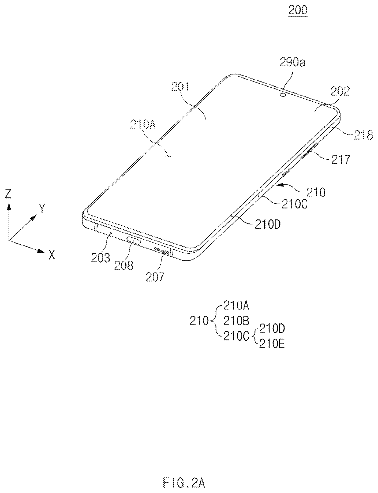
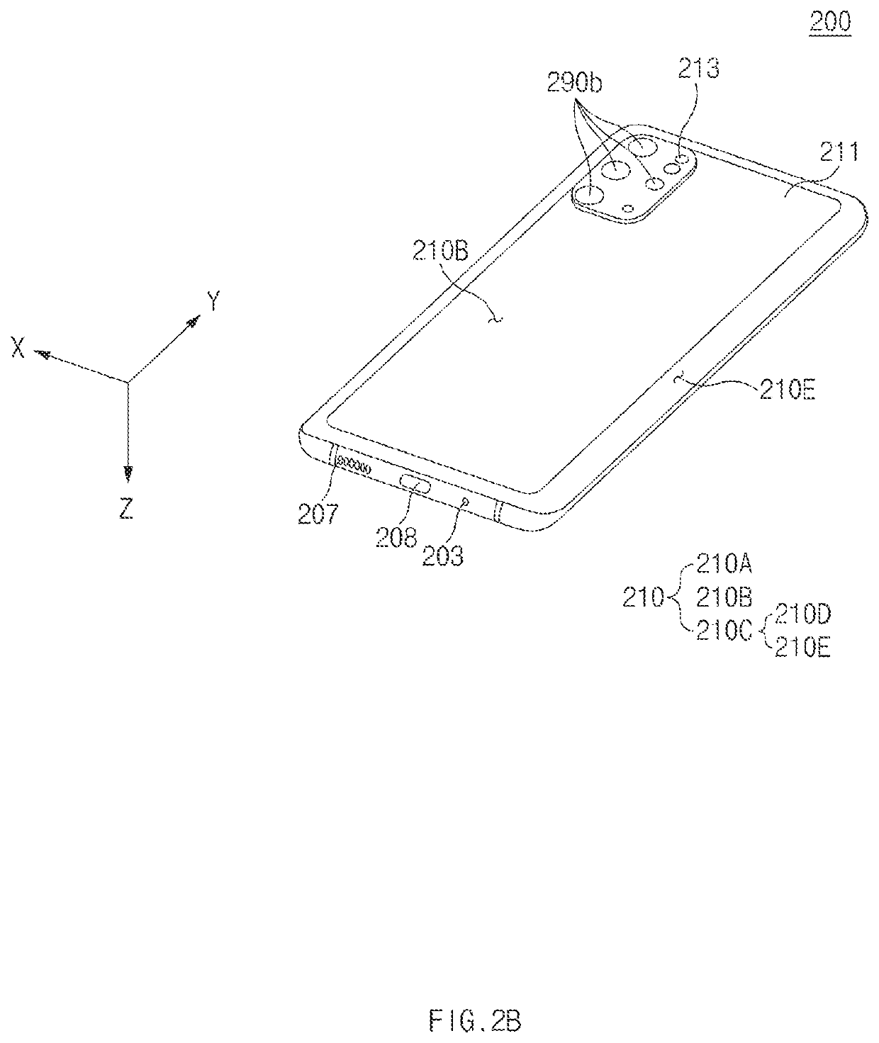
[0024]Hereinafter, various example embodiments of the disclosure may be described with reference to accompanying drawings. Accordingly, those of ordinary skill in the art will recognize that various modifications, equivalents, and / or alternatives on the various example embodiments described herein can be variously made without departing from the scope and spirit of the disclosure. With regard to description of drawings, similar components may be marked by similar reference numerals.

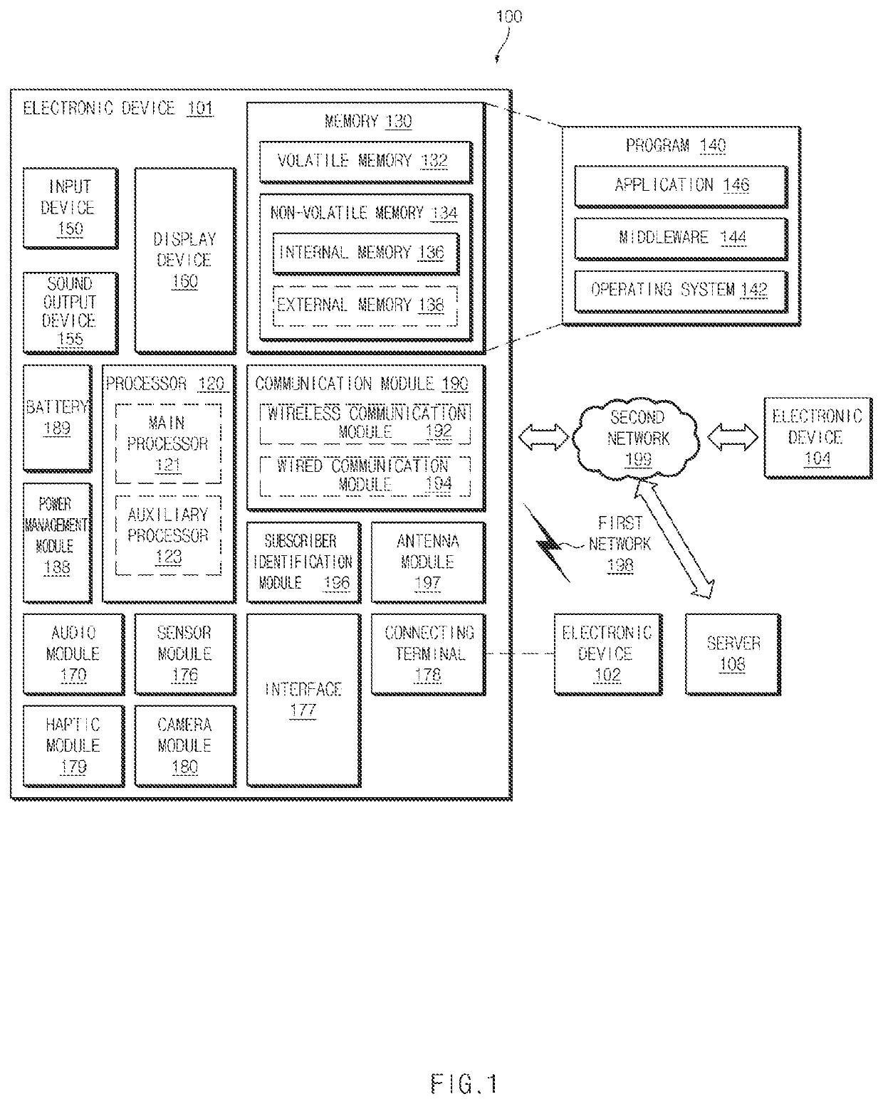
[0025]FIG. 1 is a block diagram illustrating an example electronic device 101 in a network environment 100 according to various embodiments.

[0026]Referring to FIG. 1, the electronic device 101 in the network environment 100 may communicate with an electronic device 102 via a first network 198 (e.g., a short-range wireless communication network), or an electronic device 104 or a server 108 via a second network 199 (e.g., a long-range wireless communication network). According to an embodiment, the electron...


PUM


Abstract

An electronic device includes: a housing and a printed circuit board (PCB) structure disposed in the housing. The PCB structure includes a circuit board including an opening area formed through a first surface of the circuit board and a second surface of the circuit board opposite the first surface and a conductive pattern formed in a peripheral area around the opening area, a plate disposed on the second surface of the circuit board covering the opening area, an electronic element disposed on the plate and electrically connected with the circuit board, a resin portion disposed between the plate and the circuit board and extending from the conductive pattern, the resin portion including a conductive material, and a solder portion formed between the resin portion and the plate.

Description

CROSS-REFERENCE TO RELATED APPLICATION[0001]This application is based on and claims priority under 35 U.S.C. § 119 to Korean Patent Application No. 10-2020-0015440, filed on Feb. 10, 2020, in the Korean Intellectual Property Office, the disclosure of which is incorporated by reference herein its entirety.BACKGROUND1. Field[0002]The disclosure relates to a PCB structure and an electronic device including the same.2. Description of Related Art[0003]An electronic device may include a circuit board. A plurality of electric (e.g., electronic) elements may be disposed on the circuit board, and the circuit board may include a conductive pattern that connects the plurality of electric elements. The plurality of electric elements may be electrically connected with the conductive pattern through various means.[0004]The electric elements may be mounted on the circuit board using surface mounting technology (SMT). The surface mounting technology may include soldering the electric elements to pa...

Claims


Application Information

Patent Timeline
Patent Type & Authority Patents(United States)
IPC IPC(8): H05K3/12H05K1/02H05K1/18H05K3/30
CPCH05K3/1283H05K1/0274H05K1/181H05K3/301H05K1/0271H05K2203/0405H05K2203/10H05K2201/10121H05K2201/10151H05K3/4691H05K3/3431H05K2201/10287H01L2224/73265H01L2224/48091Y02P70/50H04N23/57H04N23/54H01L2924/00014H05K1/182H05K1/111H01L23/4952H05K1/0218H04N23/51H04N23/55
Inventor JUNG, HWAJOONGKIM, MANHOKIM, TAEHWANLEE, KIHUKCHOI, YONGHWAN
Owner SAMSUNG ELECTRONICS CO LTD
Why Eureka
Try Eureka