

Method for designing a decoupling circuit
- Summary
- Abstract
- Description
- Claims
- Application Information
AI Technical Summary
Benefits of technology
Problems solved by technology
Method used
Image

Examples
Embodiment Construction
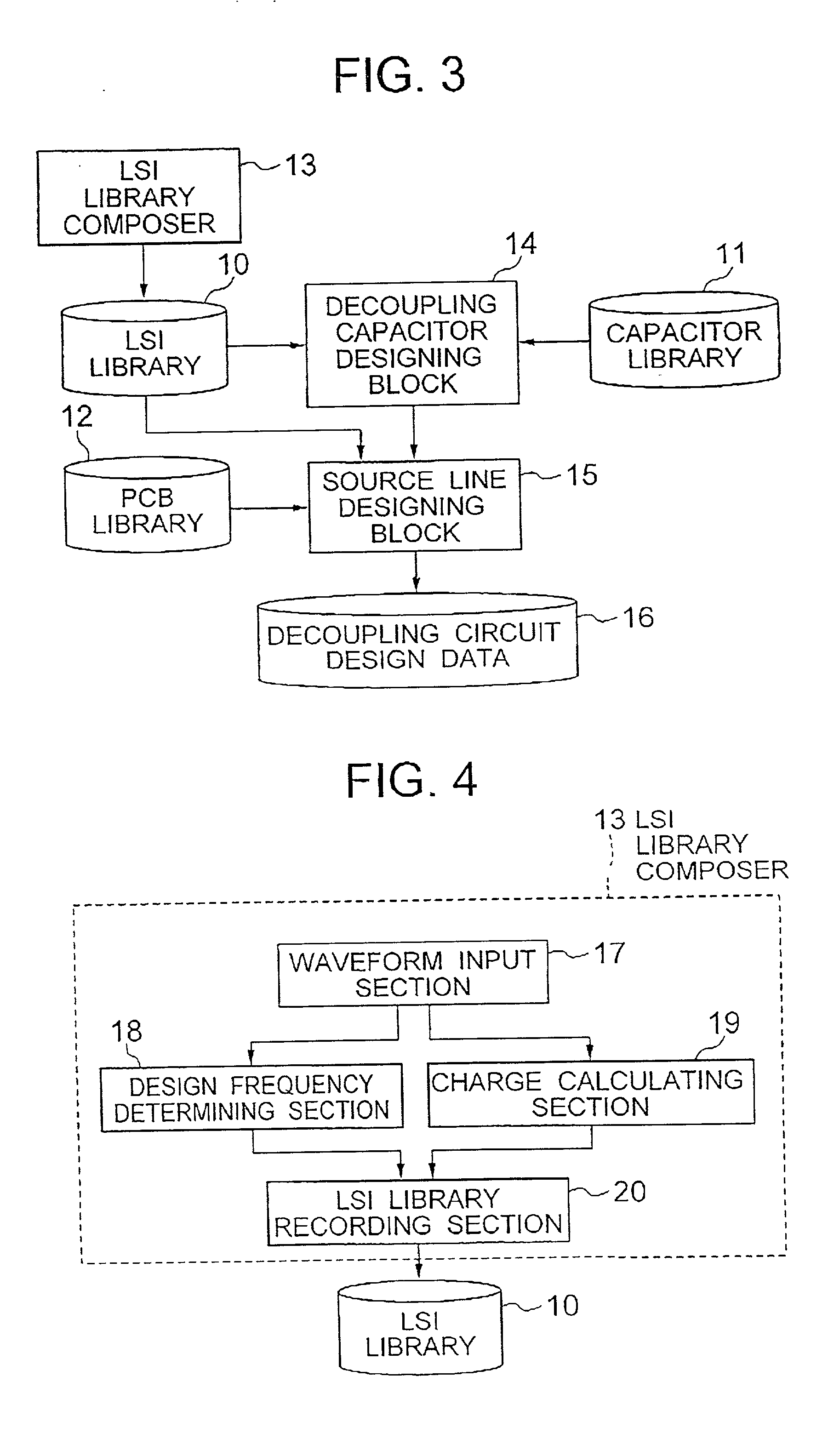
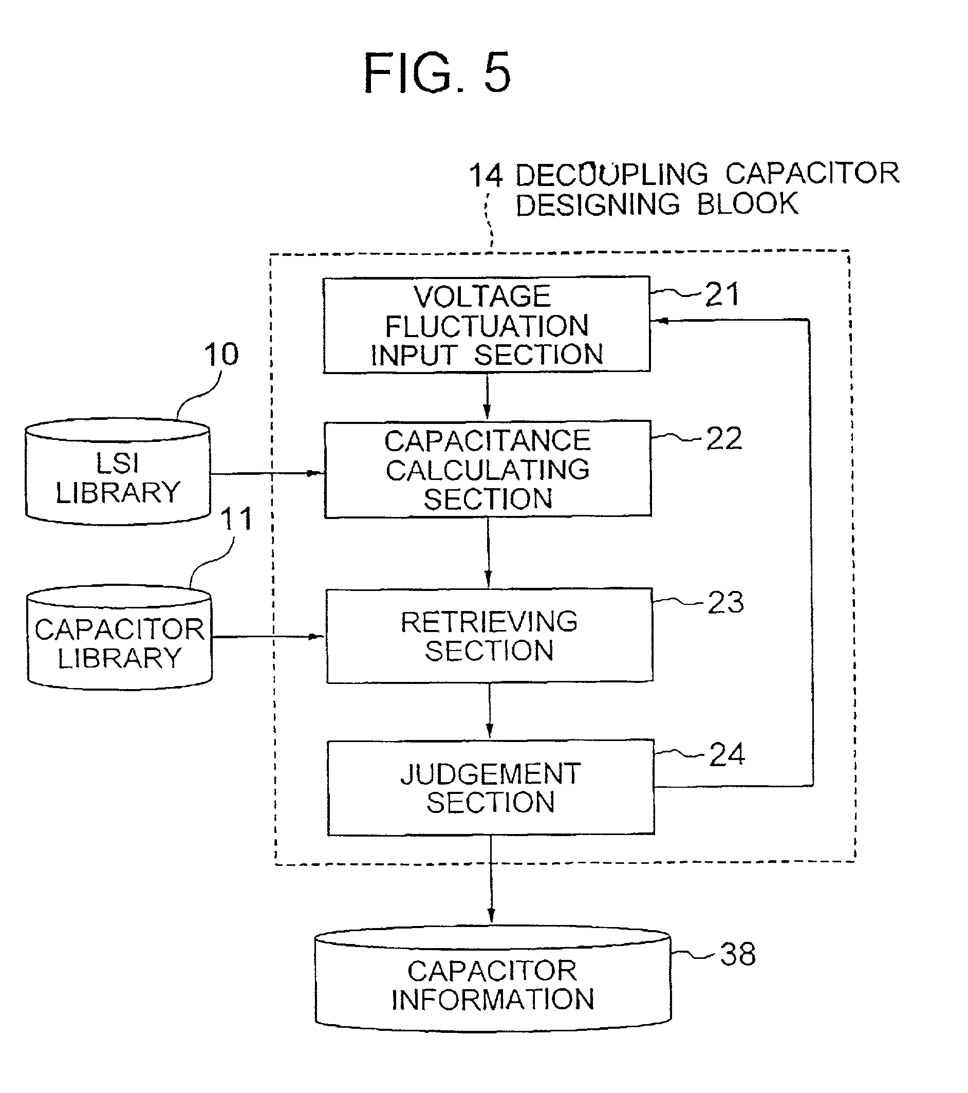
[0030] Now, the present invention is more specifically described with reference to accompanying drawings, wherein similar constituent elements are designated by similar or related reference numerals.
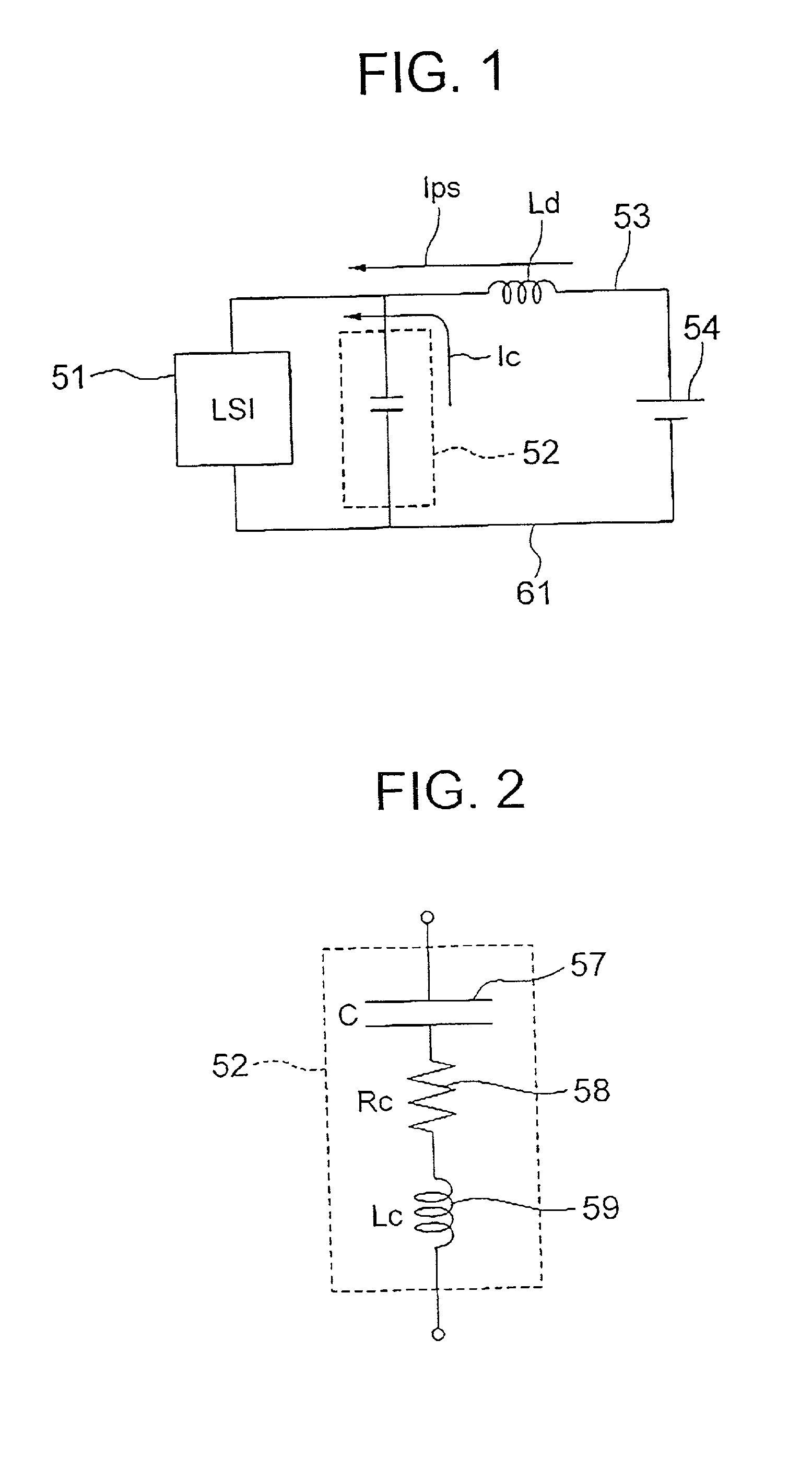
[0031] Referring to FIG. 1, a decoupling circuit for a source line to be designed by the method of the present invention includes a decoupling capacitor 52 connected in parallel with an object LSI 51 between a source line 53 and a ground line 61, and a decoupling inductor (Ld) connected in series with the LSI 51 and formed by the structure of the source line 53. The source lines 53 carries current Ips supplied from a power source 54, whereas the decoupling capacitor 52 supplies a current Ic to the LSI during a short interval of the operation thereof. The method of the present invention determines the electric parameters of the decoupling capacitor 52 and the inductor 53.
[0032] Referring to FIG. 2, the decoupling capacitor 52 shown in FIG. 1 in fact has a serial electric elements includin...
PUM
 Abstract
Description
Claims
Application Information