Device circuit of display unit

a display unit and device circuit technology, applied in static indicating devices, cathode-ray tube indicators, instruments, etc., can solve the problems of unreliable transfer of digital image data signals from the control circuit, increase in the number of wires, and inability to realistically represent the cas

Inactive Publication Date: 2001-08-23
RENESAS ELECTRONICS CORP
View PDF0 Cites 67 Cited by
  • Summary
  • Abstract
  • Description
  • Claims
  • Application Information

AI Technical Summary

Problems solved by technology

However, in such a method, the number of wires increases, so that this case is not realistic.
Therefore, if the frequency of the clock signal increased, the action of the start pulse signal (SP) between the source drivers and transfer of the digital image data signals from the control circuit becomes unreliable.
However, the transfer time for the start pulse signal (SP), that is, the period from the input of the start pulse signal to the starting of the source drivers becomes impossible to secure in accordance with the increase in speed.
Therefore, problems occur such that the digital image data signals are transmitted to the source drivers before the source drivers start operating.
That is, the action of the start pulse signal (SP) to start the source drivers becomes unreliable.
However, in the prior art 2, since the start signal generation circuits are provided for each driver, the unit becomes complicated.

Method used


Image

  • Device circuit of display unit
  • Device circuit of display unit
  • Device circuit of display unit

Examples


Embodiment Construction

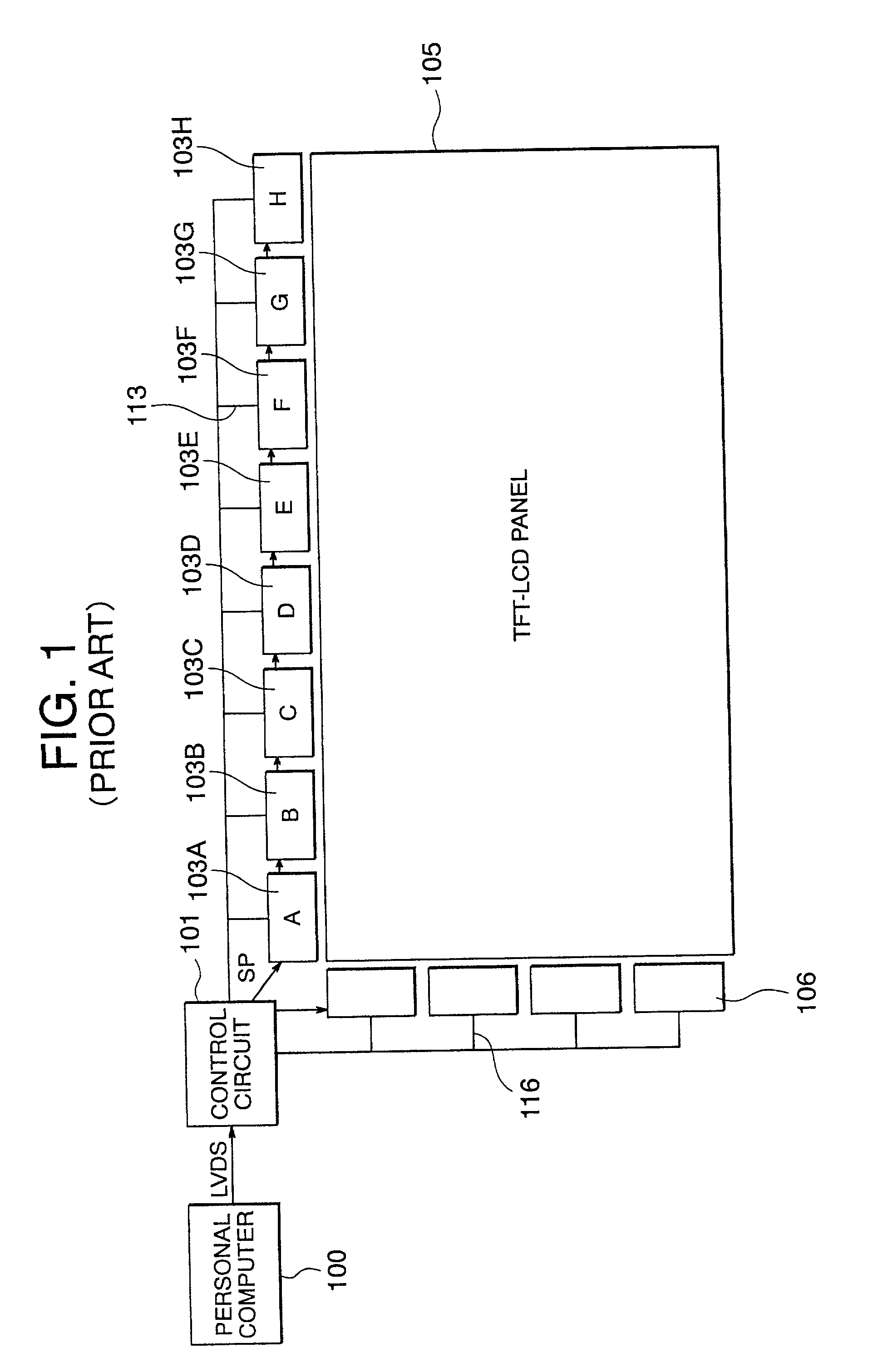
[0032] The preferred embodiments of the present invention are explained below with reference to the accompanying drawings. FIG. 4 is a circuit diagram showing a drive circuit of a display unit according to the first embodiment of the invention. In LCD panel 5, pixels are arranged in a matrix form while using a TFT as a switching device. A plurality of source drivers (a display driver) 3 are arranged along one end side in the direction of a row of the LCD panel 5. In FIG. 4, only source drivers 3A and 3B are illustrated, however, in the same manner as in FIG. 1, in actuality, 8 source drivers 3A through 3H are arranged. In addition, hereinafter, in a case where it is unnecessary to distinguish the 8 source drivers, the source drivers are referred to just as source drivers 3A through 3H, and in a case where it is necessary to distinguish the 8 source drivers, the source drivers at the 1st through 7th stages are referred to as the 1st through 7th source drivers 3A through 3G, and the s...


PUM

PropertyMeasurementUnit
sizeaaaaaaaaaa
frequencyaaaaaaaaaa
frequencyaaaaaaaaaa

Abstract

A drive circuit of a display unit has a control circuit and a plurality of source drivers that are cascade-connected to each other. A start pulse signal is inputted into the source driver at the first stage and digital image data signals and clock signals are inputted into the source drivers at the respective stages from the control circuit. Clock signals are generated by a clock control circuit of the control circuit. For the clock signals, a reading period and a transferring period appear alternately, and the frequency of the low frequency clock pulse signal in the transferring period is lower than that of the high frequency clock pulse signal in the reading period. A shift register of the source driver transfer the start pulse signal to said source driver at the next source driver within one transferring period, and the start pulse signal is thus transferred in order from the source driver at the first stage up to the source driver at the final stage. Then, the source driver inputted the start pulse signal reads the digital image data signals in the reading period.

Description

[0001] 1. Field of the Invention[0002] The present invention relates to a circuit for driving a display unit such as a liquid crystal display (LCD) for a personal computer (PC), and in particular, a drive circuit of a display unit in which clock signals are increased in speed.[0003] 2. Description of the Related Art[0004] FIG. 1 is a circuit diagram showing a conventional general drive circuit of a display unit (hereinafter, referred to as a prior art 1). As shown in FIG. 1, a plurality of source lines 113 and a plurality of gate lines 116 are formed in LCD panel 105, and at the intersection of them, pixels using a TFT (a thin-film transistor) (not shown) as a switching device are arranged in a matrix form.[0005] In FIG. 1, eight source driver LSIs (a display driver LSI) (hereinafter, referred to as a source driver) 103A through 103H to be connected to source lines 113 are arranged in a row, and four gate driver LSIs (hereinafter, referred to as gate drivers) 106 connected to the ga...

Claims


Application Information

Patent Timeline
Patent Type & Authority Applications(United States)
IPC IPC(8): G02F1/133G09G3/20G09G3/36G09G5/18
CPCG09G3/3688G09G5/18G09G2310/027G09G2370/08G09G3/36
Inventor HASHIMOTO, YOSHIHARU
Owner RENESAS ELECTRONICS CORP
Why Eureka
Try Eureka