Semiconductor raised source-drain structure

a technology of sourcedrain and semiconductors, applied in semiconductor devices, semiconductor/solid-state device details, electrical apparatus, etc., can solve the problems of difficult implanting of conductive channels, channel lack of drive and punching capability, and excessive capacitive loading from gate to source and drain

Inactive Publication Date: 2001-09-20
MICRON TECH INC
View PDF0 Cites 14 Cited by
  • Summary
  • Abstract
  • Description
  • Claims
  • Application Information

AI Technical Summary

Benefits of technology

0007] The present invention is directed to a semiconductor structure which includes a raised source and a raised drain. The structure also includes a g

Problems solved by technology

Such an isolation arrangement, however, can cause excessive capacitive loading from gate to source and drain.
Such channels do not have good drive and pu

Method used


Image

  • Semiconductor raised source-drain structure
  • Semiconductor raised source-drain structure
  • Semiconductor raised source-drain structure

Examples


Embodiment Construction

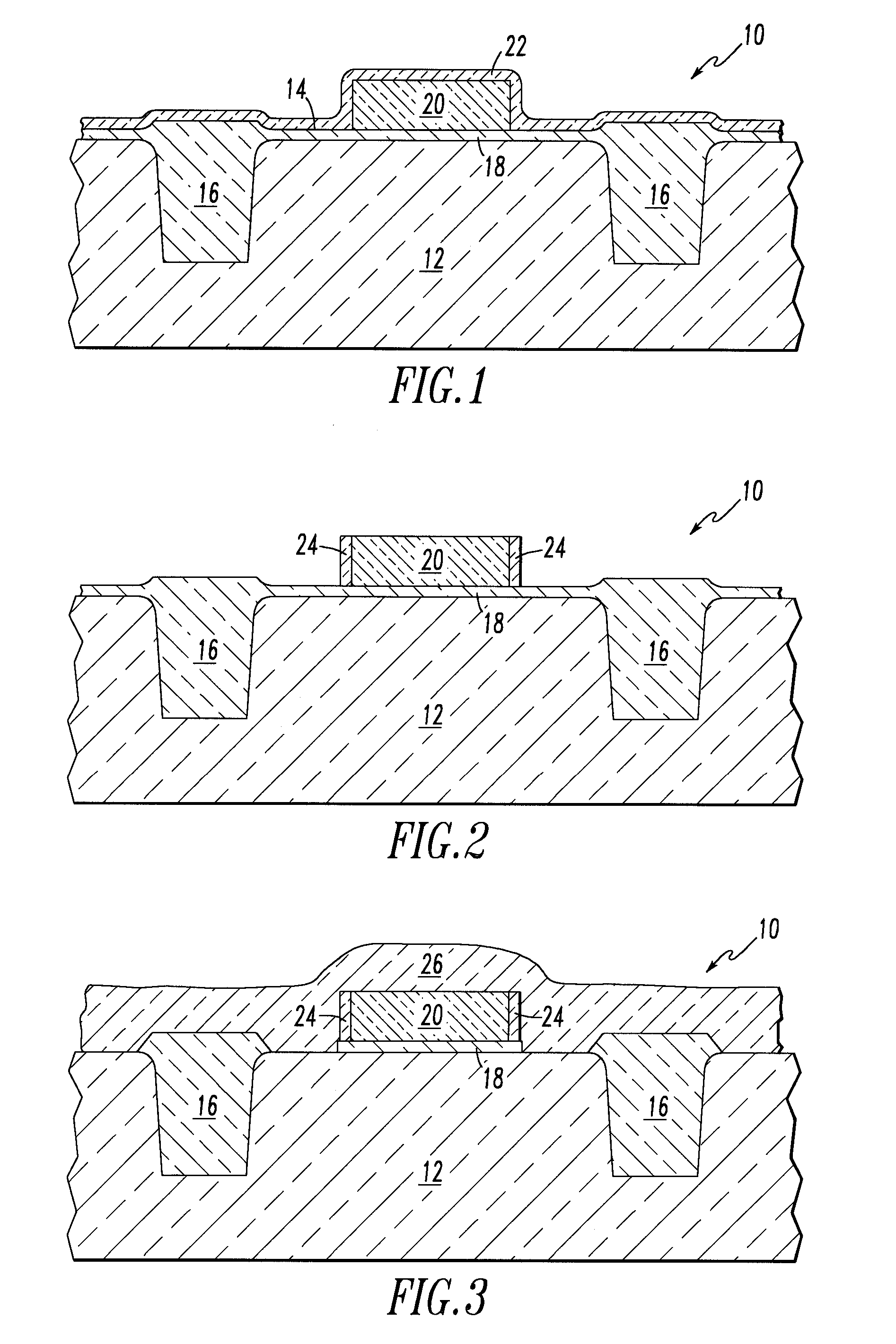
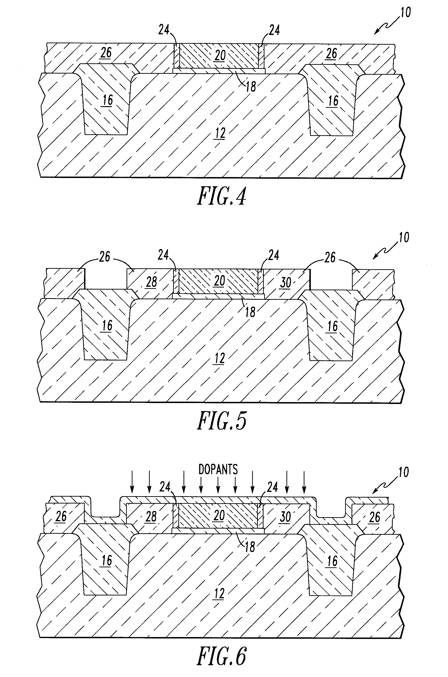
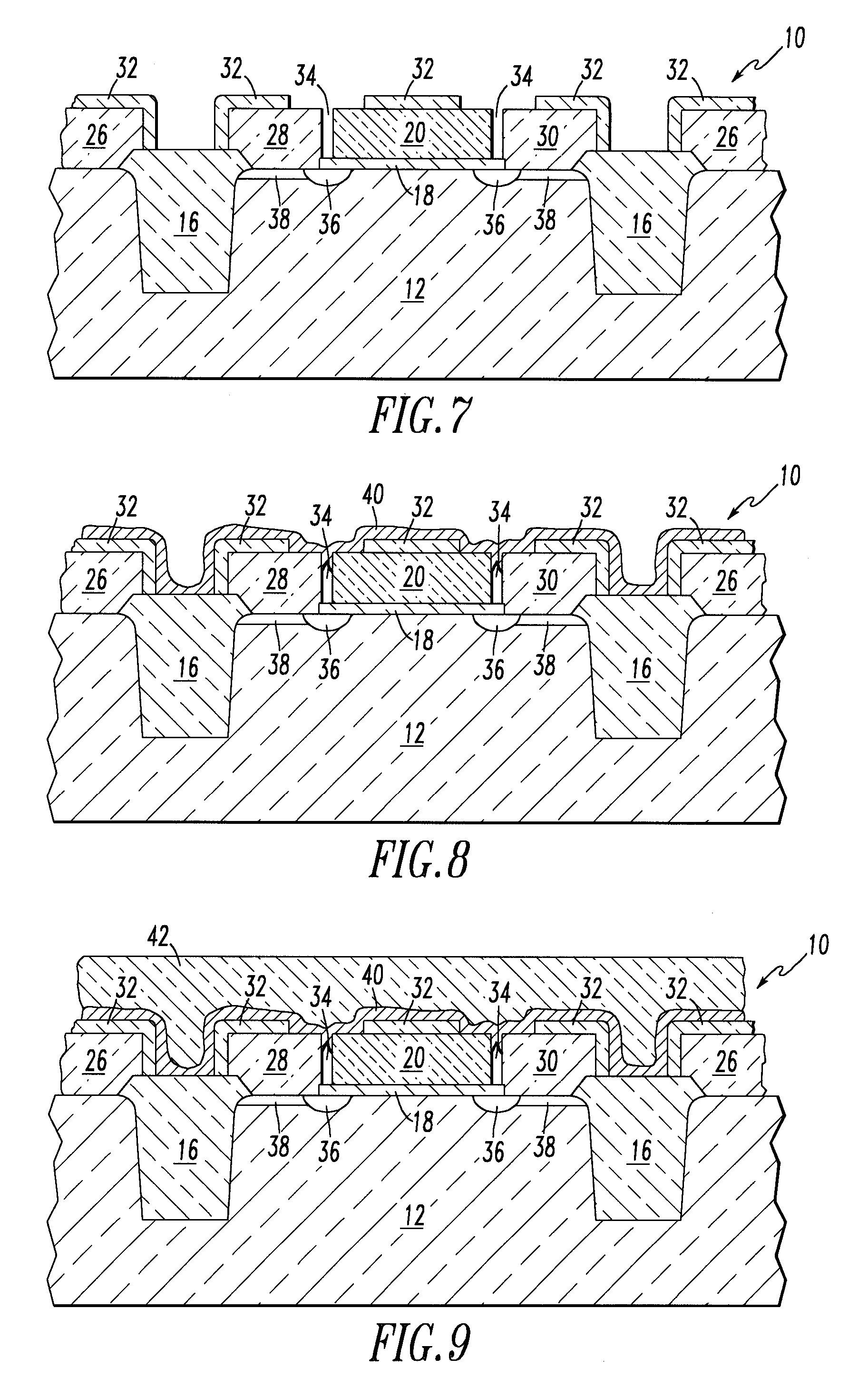
[0023] It is to be understood that the figures and descriptions of the present invention have been simplified to illustrate elements and process steps that are relevant for a clear understanding of the present invention, while eliminating, for purposes of clarity, other elements and process steps found in a typical semiconductor topography. For example, specific methods and steps of removing layers or portions of layers using techniques such as lithography and etching are not described. Those of ordinary skill in the art will recognize that other elements and process steps are desirable and / or required to produce an operational device incorporating the present invention. However, because such elements and process steps are well known in the art, and because they do not facilitate a better understanding of the present invention, a discussion of such elements and process steps is not provided herein.

[0024] FIG. 1 is a cross-sectional view of a substrate assembly 10 at an early stage o...


PUM


Abstract

<heading lvl="0">Abstract of Disclosure</heading> A semiconductor structure which includes a raised source and a raised drain. The structure also includes a gate located between the source and drains. The gate defines a first gap between the gate and the source and a second gap between the gate and the drain.

Description

Background of Invention[0001] Field of the Invention[0002] The present invention is directed generally to a semiconductor raised source-drain structure and, more particularly, to a semiconductor raised source-drain structure with gate side gaps and pocket junctions.[0003] Description of the Background[0004] Raised source and drains have been demonstrated in submicron semiconductor devices. In contrast to conventional source and drains, raised source and drains are vertical structures formed on top of the substrate instead of implanted structures in the substrate surface. Thin film structures are typically inserted between the sidewalls of the gate and the top regions of the raised source and drains to isolate the gate from the source and drains. Such an isolation arrangement, however, can cause excessive capacitive loading from gate to source and drain.[0005] Devices incorporating raised source and drains typically include implanted n- regions under the source and drain regions to c...

Claims


Application Information

Patent Timeline
IPC IPC(8): H01L21/285H01L21/336H01L21/768H01L23/522H01L29/417H01L29/49
CPCH01L21/28512H01L21/7682H01L21/76895H01L23/5226H01L29/41775H01L29/41783H01L29/4983H01L29/4991H01L29/66492H01L2924/0002H01L2924/00
Inventor GONZALEZ , FERNANDOMOULI , CHANDRA
Owner MICRON TECH INC
Why Eureka
Try Eureka