Comparator for determining process variations

a technology of process variation and comparator, which is applied in the field of comparator for determining process variations, can solve the problems of increasing memory speed, increasing memory cost, and reducing the dimensions of individual elements of the semiconductor device,

a technology of process variation and comparator, which is applied in the field of comparator for determining process variations, can solve the problems of increasing memory speed, increasing memory cost, and reducing the dimensions of individual elements of the semiconductor device,

US20020021158A1Inactive Publication Date: 2002-02-21MICRON TECH INC

Image

  • Comparator for determining process variations
  • Comparator for determining process variations
  • Comparator for determining process variations

Examples


Embodiment Construction

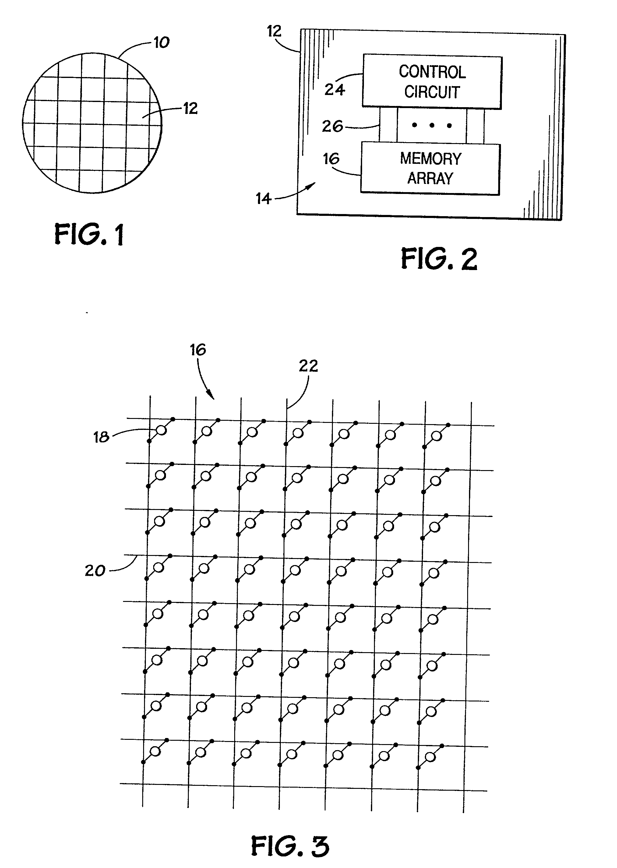
[0025] Turning now to the drawings, and referring initially to FIG. 1, a substrate, such as a semiconductor wafer, is illustrated and generally designated by the reference numeral 10. The wafer has been partitioned into a plurality of die 12. Typically, use of the die 12 contains an integrated circuit that is substantially identical to the integrated circuit contained by each of the other die 12 on the wafer 10.

[0026] Although a wide variety of integrated circuits may be formed on the die 12 of the wafer 10, in the embodiment illustrated in FIG. 2, a semiconductor memory device 14, such as a DRAM, is formed on the die 12. The memory device 14 generally includes a memory array 16. As illustrated in FIG. 3, the memory array 16 typically includes a plurality of memory cells 18 that are arranged in multiple rows and multiple columns. Each of the memory cells 18 is coupled to a respective row line 20 and to a respective column line 22. The memory device 14 also includes a control circuit...


PUM


Abstract

A comparison circuit may be fabricated along with a primary circuit on a semiconductor substrate. The propagation delay of a comparison signal across a first path of circuit elements is compared to propagation delays of the comparison signal across a second path of delay elements. As a semiconductor fabrication process varies, the relative propagation delays across the first and second paths will vary in a manner correlative to the process variations. By monitoring the relative propagation delays, the fabrication process may be controlled to ensure that the process does not vary to an undesirable extent. Also, various programmable delay elements may be fabricated into the primary circuit, and these programmable delay elements may be activated and / or deactivated in response to the relative propagation delays of the comparison circuit.

Description

[0001] 1. Field of the Invention[0002] The present invention relates generally to electronic circuitry and, more particularly, to a method and apparatus for comparing signal propagation delay across one circuit path with signal propagation delay across another circuit path.[0003] 2. Description of the Related Art[0004] This section is intended to introduce the reader to various aspects of art which may be related to various aspects of the present invention which are described and / or claimed below. This discussion is believed to be helpful in providing the reader with background information to facilitate a better understanding of the various aspects of the present invention. Accordingly, it should be understood that these statements are to be read in this light, and not as admissions of prior art.[0005] Microprocessor-controlled integrated circuits are used in a wide variety of applications. Such applications include personal computers, vehicle control systems, telephone networks, an...

Claims


Application Information

Patent Timeline
21 Feb 2002
Publication
US20020021158A1
IPC
H03K5/159; H03K5/26; H03K19/003
CPC
H03K5/159; H03K5/26; H03K19/00323
Inventors
MULLARKEY, PATRICK J.